2 layers100 × 77.5 mm

 jimbro1000/BaderVGA
prototype very bad vga for SBC6309
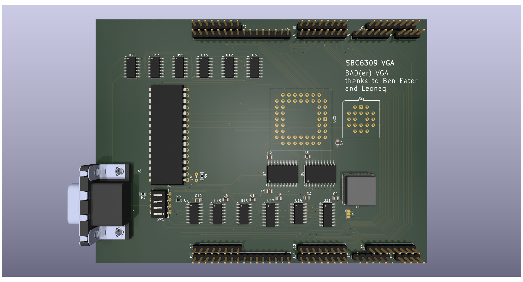
BadVga is an open-source printed circuit board by jimbro1000, from the jimbro1000/BaderVGA repository on GitHub. It is a 4-layer board of 139.3 × 102.4 mm with 49 parts on 159 nets, routed with 1,578 tracks and 203 vias.
It is built around the 74HC245D, 74LS30PC and 74LS00SC, with the 74LS20P-E and CD74HC4040E among its other parts. Its parts include 17 ICs, 15 connectors, 10 capacitors, 3 resistors and 1 switch. It belongs with the FPGA and CPLD boards of this library.


Inspired by Ben Eater's discrete logic VGA and Leoneq's "bad vga" design, this project implements a very basic, text only VGA display using just 1 bit of a 128KB EEPROM data bus and 2KB of SRAM.
The logic chips used are clocked to near their limit (notably the 12-bit counters) and struggle to meet the timing requirements of the design. Careful selection of components should help to resolve this.
The original designs by Ben and Leoneq were built on breadboard with no practical ground plane and very little decoupling. This design is a dedicated 4-layer PCB with two solid ground planes that should help to resolve the problem. As much as possible, all signals are routed on a single layer with the "spare" layer used for power delivery.
Timing is not just an issue for the board's clock it is also a problem for the host. The board clock is decoupled from the host which will, inevitably, result in read and write conflicts. The host is expected to be running at 3.147MHz while the video board is running at 20MHz. It should be viable to gate host r/w operations such that they are blocked (in the semaphore sense) by the video. If not the only option is to restrict write operations to the vertical blank period. The alternative is to switch to a dual-port arrangement and bypass the problem completely.
Integration with the host requires address bus, data bus, enable/select and R/!W.
Outputs from the board, by default, are just the data bus but this needs to be extended to include horizontal and vertical sync (TODO)
Ben Eater VGA https://eater.net/vga
Leoneq https://github.com/Leoneq/iNapGPU
Dr Matt Regan VGA https://github.com/Turing6502/ZX-Spectrum-No-ULA/blob/main/ZX%20Spectrum%20No%20ULA.pdf
This project is licensed under CC BY-SA 4.0 https://creativecommons.org/licenses/by-sa/4.0/
| Qty | Value | Footprint | References |
|---|---|---|---|
| 10 | 10nF | Capacitor_SMD:C_0805_2012Metric | C1, C2, C3, C4, C5, C6, C7, C8, C9, C10 |
| 8 | Conn_01x08 | Connector_PinHeader_2.54mm:PinHeader_1x08_P2.54mm_Vertical | J4, J5, J7, J9, J12, J13, J14, J15 |
| 5 | 74LS30 | Package_SO:SOIC-14_3.9x8.7mm_P1.27mm | U7, U14, U15, U18, U19 |
| 3 | 74LS00 | Package_SO:SOIC-14_3.9x8.7mm_P1.27mm | U3, U16, U20 |
| 2 | 10K | PCM_Resistor_SMD_AKL:R_0603_1608Metric | R3, R4 |
| 2 | 74HC245 | Package_SO:SOIC-20W_7.5x12.8mm_P1.27mm | U2, U8 |
| 2 | 74LS20 | Package_SO:SOIC-14_3.9x8.7mm_P1.27mm | U12, U13 |
| 2 | CD74HC4040 | Package_SO:SOIC-16_3.9x9.9mm_P1.27mm | U11, U17 |
| 2 | Conn_01x04 | Connector_PinHeader_2.54mm:PinHeader_1x04_P2.54mm_Vertical | J6, J10 |
| 2 | Conn_01x06 | Connector_PinHeader_2.54mm:PinHeader_1x06_P2.54mm_Vertical | J2, J8 |
| 2 | Conn_01x16 | Connector_PinHeader_2.54mm:PinHeader_1x16_P2.54mm_Vertical | J3, J16 |
| 1 | 1K | PCM_Resistor_SMD_AKL:R_0603_1608Metric | R5 |
| 1 | 27C010 | Package_DIP:DIP-32_W15.24mm | U1 |
| 1 | GAL16V8 | Package_LCC:PLCC-20_THT-Socket | U22 |
| 1 | IDT71342 | Package_LCC:PLCC-52_THT-Socket | U21 |
| 1 | SW_DIP_x04 | Button_Switch_THT:SW_DIP_SPSTx04_Slide_6.7x11.72mm_W7.62mm_P2.54mm_LowProfile | SW1 |
| 1 | TFT660 | Oscillator:Oscillator_DIP-8 | Y1 |
| 1 | VGA | Library:AMPHENOL_ICD15S13E4GX00LF | J1 |
| 1 | ZWORKA | PCM_Jumper_AKL:Jumper_P2.54mm_D0.7mm | JP1 |
| 1 | videoclock source | Jumper:SolderJumper-3_P1.3mm_Bridged12_Pad1.0x1.5mm | JP2 |


kev-ju/PC-Retro-MTM
Modern KiCad version of the IBM 5150 system board originally created by MTM Scientific, Inc.

ForgottenMachines/Entrex
The technologies documented here will include all like-kind systems manufactured by Nixdorf, Redifon, ROCC & Mera, all originally designed by Entrex Inc, Burlington, MA USA.

jimbro1000/DIY-Video
General purpose video system for 8-bit computers using 74LS logic

roberto314/GIMIX_reproduction
Reproducing SS-50 and SS-30 cards and GIMIX Ghost Case and Mainboard

CPTforever/8088-MicroATX-Computer
A 8088 based, IBM 5150 like computer compatible with the MicroATX motherboard form factor.
It measures 139.3 × 102.4 mm and has 4 copper layers, 1.6 mm thick.
49 parts, built around the 74HC245D, 74LS30PC, 74LS00SC and 74LS20P-E. The full list of its parts is on this page, with links to each part's symbol and footprint where PCBKit's library has them.
From the jimbro1000/BaderVGA repository on GitHub, at the commit this page was made from: the board is badVga.kicad_pcb and its schematic badVga.kicad_sch. PCBKit opens the board in the browser, with nothing to install.
Its repository states no licence, so its author keeps all rights: ask jimbro1000 before reusing the design.