2 layers140 × 90 mm
 jdg511/GAS
KiCad 10 is installed locally on this machine.
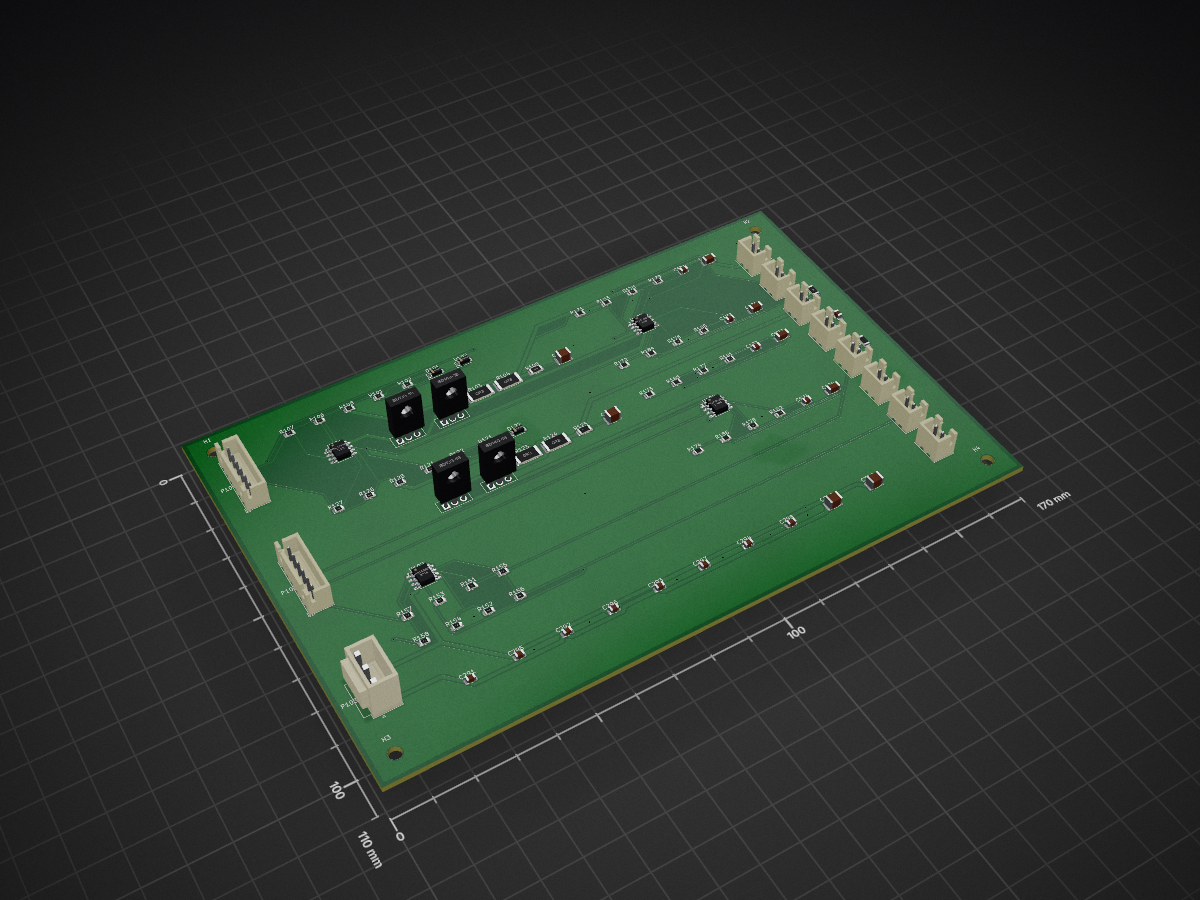
Tank driver recovery is an open-source printed circuit board by jdg511, from the jdg511/GAS repository on GitHub. It is a 2-layer board of 170 × 110 mm with 90 parts on 51 nets, routed with 489 tracks and 52 vias.
It is built around the 1N4148W, BD139-16 and BD140-16. Its parts include 42 resistors, 21 capacitors, 11 connectors, 4 ICs and 4 diodes.


KiCad 10 is installed locally on this machine.
This folder is the intended home for the hardware project once schematic capture starts.
GAS-Hardware.kicad_proGAS-Hardware.kicad_schThe KiCad project now has a real top-level hierarchical shell, first-pass real symbol capture across every rev-A child sheet, and a first-pass electrically assigned power/backplane page.
What currently exists:
power-backplane.kicad_schWhat does not yet exist:
Capture should now key off:
During this session, the hierarchical top-level shell and all child sheets were accepted by kicad-cli, and the release-export script still produced schematic PDFs successfully after the interface-label pass.
Important current nuance:
kicad-cli sch export pdf still succeedsCurrent exported folder:
hardware/kicad/exportsRepeatable release/export helper:
Repeatable capture-progress audit:
Run:
python hardware/kicad/audit-rev-a-capture.pyCurrent baseline from the latest 2026-06-29 audit:
6 / 6 child sheets present88 / 8882 / 82Current release-export / ERC baseline from the same session:
88 / 88 planned refs present and 82 / 82 manifest labels present650 known intermediate violations after the I/O-board center-short cleanup pass on 2026-06-29404 to 376 local violations in the same pass, and its multiple-net-name collisions dropped from 8 to 2WD_L_LO <-> WET_SUM_L and WD_R_LO <-> WET_SUM_R wet-return aliasesCurrent PCB scaffold baseline:
crossfade-feedback-wet.kicad_pcb: 100 mm x 70 mm, 8 electrical footprints, 4x M3 mounting holes, DRC cleanext-tank-routing.kicad_pcb: 120 mm x 80 mm, 12 electrical footprints, 4x M3 mounting holes, DRC cleanfilter-clipper.kicad_pcb: 140 mm x 90 mm, 19 electrical footprints, 4x M3 mounting holes, DRC cleanio-board.kicad_pcb: 160 mm x 75 mm, 50 electrical footprints, 4x M3 mounting holes, DRC cleanpower-backplane.kicad_pcb: 150 mm x 95 mm, 14 electrical footprints, 4x M3 mounting holes, DRC cleantank-driver-recovery.kicad_pcb: 170 mm x 110 mm, 11 electrical footprints, 4x M3 mounting holes, DRC cleanRepeatable PCB footprint placement helper:
Current scripted output root:
hardware/kicad/release-exports/rev-a-releaseBefore ordering boards, run:
.\hardware\kicad\test-rev-a-order-readiness.ps1The gate writes:
It intentionally fails while any of these are true:
*.kicad_pcb board layout files existThe current project is therefore not order-ready. It remains in schematic-capture cleanup before PCB layout, DRC, Gerber/drill export, and simulation setup.
BOM.csv| Qty | Value | Footprint | References |
|---|---|---|---|
| 8 | 100n | Capacitor_SMD:C_0805_2012Metric | C291, C292, C293, C294, C295, C296, C297, C298 |
| 8 | 10k | Resistor_SMD:R_0805_2012Metric | R107, R108, R127, R128, R153, R154, R157, R158 |
| 6 | 1k | Resistor_SMD:R_0805_2012Metric | R106, R126, R175, R176, R177, R178 |
| 4 | 0 | Resistor_SMD:R_0805_2012Metric | R183, R184, R185, R186 |
| 4 | 0.33 | Resistor_SMD:R_2512_6332Metric | R103, R104, R123, R124 |
| 4 | 1N4148W | Diode_SMD:D_SOD-123 | D101, D102, D121, D122 |
| 4 | 2.2Meg | Resistor_SMD:R_0805_2012Metric | R171, R172, R173, R174 |
| 4 | 22n | Capacitor_SMD:C_1206_3216Metric | C175, C176, C177, C178 |
| 4 | 33k | Resistor_SMD:R_0805_2012Metric | R179, R180, R181, R182 |
| 4 | 68 | Resistor_SMD:R_0805_2012Metric | R101, R102, R121, R122 |
| 4 | 68p | Capacitor_SMD:C_0805_2012Metric | C171, C172, C173, C174 |
| 4 | M3 | MountingHole:MountingHole_3.2mm_M3 | H1, H2, H3, H4 |
| 4 | OPA1656IDR | Package_SO:SOIC-8_3.9x4.9mm_P1.27mm | U101, U102, U103, U104 |
| 2 | 10 | Resistor_SMD:R_1206_3216Metric | R105, R125 |
| 2 | 12k | Resistor_SMD:R_0805_2012Metric | R151, R152 |
| 2 | 220 | Resistor_SMD:R_0805_2012Metric | R155, R156 |
| 2 | 22u | Capacitor_SMD:C_1210_3225Metric | C299, C300 |
| 2 | 47n | Capacitor_SMD:C_1210_3225Metric | C101, C121 |
| 2 | BD139-16 | Package_TO_SOT_THT:TO-126-3_Vertical | Q101, Q103 |
| 2 | BD140-16 | Package_TO_SOT_THT:TO-126-3_Vertical | Q102, Q104 |
| 1 | 0 | Resistor_SMD:R_1206_3216Metric | R206 |
| 1 | 100 | Resistor_SMD:R_1206_3216Metric | R205 |
| 1 | 1n | Capacitor_SMD:C_0805_2012Metric | C191 |
| 1 | JTR-PRI B6B-XH-A | Connector_JST:JST_XH_B6B-XH-A_1x06_P2.50mm_Vertical | P101 |
| 1 | JTR-PWR B3P-VH-B | Connector_JST:JST_VH_B3P-VH_1x03_P3.96mm_Vertical | P103 |
| 1 | JTR-SEC B6B-XH-A | Connector_JST:JST_XH_B6B-XH-A_1x06_P2.50mm_Vertical | P102 |
| 1 | PRI L RET | Connector_JST:JST_XH_B2B-XH-A_1x02_P2.50mm_Vertical | J102 |
| 1 | PRI L SEND | Connector_JST:JST_XH_B2B-XH-A_1x02_P2.50mm_Vertical | J101 |
| 1 | PRI R RET | Connector_JST:JST_XH_B2B-XH-A_1x02_P2.50mm_Vertical | J104 |
| 1 | PRI R SEND | Connector_JST:JST_XH_B2B-XH-A_1x02_P2.50mm_Vertical | J103 |
| 1 | SEC L RET | Connector_JST:JST_XH_B2B-XH-A_1x02_P2.50mm_Vertical | J106 |
| 1 | SEC L SEND | Connector_JST:JST_XH_B2B-XH-A_1x02_P2.50mm_Vertical | J105 |
| 1 | SEC R RET | Connector_JST:JST_XH_B2B-XH-A_1x02_P2.50mm_Vertical | J108 |
| 1 | SEC R SEND | Connector_JST:JST_XH_B2B-XH-A_1x02_P2.50mm_Vertical | J107 |


khomyakova228-cell/pulse-oximeter
Домашнее задание по курсу «САПР электронных средств» «Проект печатного узла пульсоксиметра в KiCad: оформление по ГОСТ, библиотека компонентов, автоматизация проверки и выпуска» Обозначение документа: БИГЕ.149980.001 Э3


fossasia/pslab-hardware
PSLab Hardware Design and Schematics https://pslab.io

pierrechevalier83/ferris
A low profile split keyboard designed to satisfy one single use case elegantly


It measures 170 × 110 mm and has 2 copper layers, 1.6 mm thick.
90 parts, built around the 1N4148W, BD139-16 and BD140-16. The full list of its parts is on this page, with links to each part's symbol and footprint where PCBKit's library has them.
From the jdg511/GAS repository on GitHub, at the commit this page was made from: the board is hardware/kicad/tank-driver-recovery.kicad_pcb and its schematic hardware/kicad/archive/abandoned-top-level/GAS-Hardware.kicad_sch. PCBKit opens the board in the browser, with nothing to install.
Its repository states no licence, so its author keeps all rights: ask jdg511 before reusing the design.