2 layers75 × 64 mm

 jbteja/tj03-usb-micro-programmer
USB Micro Programmer for ESP and Arduino Boards
Usb micro programmer is an open-source printed circuit board by jbteja, from the jbteja/tj03-usb-micro-programmer repository on GitHub, published under the MIT licence. It is a 2-layer board of 60 × 30 mm with 38 parts on 27 nets, routed with 241 tracks and 35 vias.
It is built around the AMS1117-3.3, MMSS8050-H-TP and 1N4007-T, with the SP0503BAHTG among its other parts. Its parts include 9 capacitors, 5 resistors, 4 connectors, 3 inductors and 2 ICs. It belongs with the interfaces and adapters boards of this library.


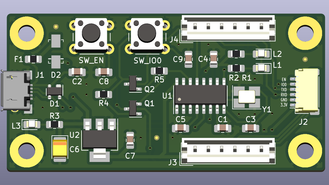
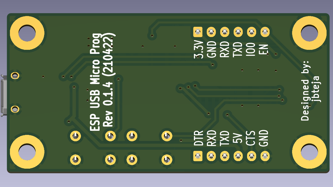
Image of the programmer:
| Qty | Value | Footprint | References |
|---|---|---|---|
| 4 | 0.1uF | Capacitor_SMD:C_0805_2012Metric_Pad1.18x1.45mm_HandSolder | C2, C4, C8, C9 |
| 4 | MountingHole | MountingHole:MountingHole_3.2mm_M3_Pad | H1, H2, H3, H4 |
| 3 | Fiducial | Fiducial:Fiducial_0.5mm_Mask1mm | FID1, FID2, FID3 |
| 2 | 10k | Resistor_SMD:R_0805_2012Metric_Pad1.20x1.40mm_HandSolder | R4, R5 |
| 2 | 1K | Resistor_SMD:R_0805_2012Metric_Pad1.20x1.40mm_HandSolder | R1, R2 |
| 2 | 22pF | Capacitor_SMD:C_0805_2012Metric_Pad1.18x1.45mm_HandSolder | C1, C3 |
| 2 | RED | LED_SMD:LED_0805_2012Metric_Pad1.15x1.40mm_HandSolder | L1, L3 |
| 2 | S8050(NPN) | Package_TO_SOT_SMD:SOT-23 | Q1, Q2 |
| 2 | SW_Push | Button_Switch_THT:SW_PUSH_6mm_H5mm | SW_EN, SW_IO0 |
| 1 | 0.5A | Fuse:Fuse_0805_2012Metric_Pad1.15x1.40mm_HandSolder | F1 |
| 1 | 10nF | Capacitor_SMD:C_0805_2012Metric_Pad1.18x1.45mm_HandSolder | C5 |
| 1 | 12MHz | Crystal:Crystal_SMD_3225-4Pin_3.2x2.5mm_HandSoldering | Y1 |
| 1 | 1N4007 | digikey-footprints:DO-214AC | D2 |
| 1 | 22uF/25V | Capacitor_SMD:C_0805_2012Metric_Pad1.18x1.45mm_HandSolder | C7 |
| 1 | 22uF/25V | Capacitor_Tantalum_SMD:CP_EIA-3528-21_Kemet-B_Pad1.50x2.35mm_HandSolder | C6 |
| 1 | 2K | Resistor_SMD:R_0805_2012Metric_Pad1.20x1.40mm_HandSolder | R3 |
| 1 | AMS1117-3.3 | Package_TO_SOT_SMD:SOT-223-3_TabPin2 | U2 |
| 1 | CH340C/G | Package_SO:SOIC-16_3.9x9.9mm_P1.27mm | U1 |
| 1 | ESP_Link | Connector_JST:JST_SH_SM06B-SRSS-TB_1x06-1MP_P1.00mm_Horizontal | J2 |
| 1 | ESP_Prog | Connector_JST:JST_EH_B6B-EH-A_1x06_P2.50mm_Vertical | J3 |
| 1 | SP0503BAHT | Package_TO_SOT_SMD:SOT-143 | D1 |
| 1 | Standard_Prog | Connector_JST:JST_EH_B6B-EH-A_1x06_P2.50mm_Vertical | J4 |
| 1 | USB_B_Micro | digikey-footprints:USB_Micro_B_Female_10118193-0001LF | J1 |
| 1 | YELLOW | LED_SMD:LED_0805_2012Metric_Pad1.15x1.40mm_HandSolder | L2 |
It measures 60 × 30 mm and has 2 copper layers, 1.6 mm thick.
38 parts, built around the AMS1117-3.3, MMSS8050-H-TP, 1N4007-T and SP0503BAHTG. The full list of its parts is on this page, with links to each part's symbol and footprint where PCBKit's library has them.
From the jbteja/tj03-usb-micro-programmer repository on GitHub, at the commit this page was made from: the board is usb-micro-programmer.kicad_pcb and its schematic usb-micro-programmer.kicad_sch. PCBKit opens the board in the browser, with nothing to install.
Its repository publishes it under the MIT licence: you may reuse it on that licence's terms (keep the author's notice, and for a copyleft licence share your changes alike).


alejomancinelli/FCEIA_ProyectoFinal
Proyecto Final de Ing. Electrónica: Sistema de monitoreo de red eléctrica doméstica y/o industrial


futureshocked/KLP3e_ESP32_development_kit
This is the repository for the "ESP32 Devkit clone" project.

futureshocked/KLP4e_ESP32-Clone-Devkit
This is the repository for the "ESP32 devikit clone" project.

Purdue-Northwest-Vibration-Anaylsis/Purdue-Northwest-Vibration-Analysis
Vibration analysis senior design project for purdue northwest.