2 layers49.5 × 49.7 mm
AudioPowerBoard
LEAT-EDGE/ambient-pcb-audiopower
Audio capture and energy management daughterboard PCB for the Ambient project.
121 partsCERN-OHL-P-2.0
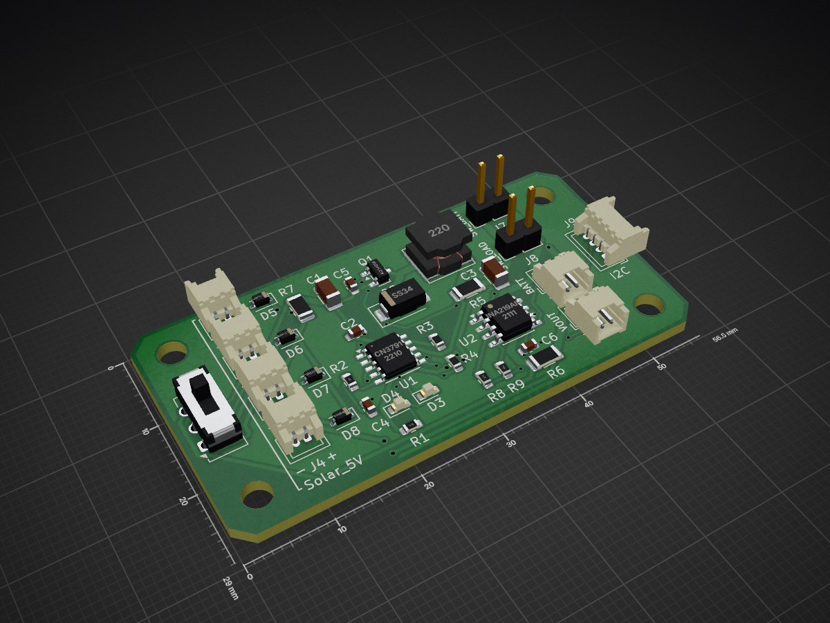
 jaisor/SolarNodeChargeController
KiCad 10 solar 1S LiPo charger: CN3791 MPPT, up to 4x 5V panels, INA219 I2C power monitor
SolarNodeChargeController is an open-source printed circuit board by jaisor, from the jaisor/SolarNodeChargeController repository on GitHub. It is a 2-layer board of 56.5 × 29 mm with 40 parts on 26 nets, routed with 208 tracks and 45 vias.
It is built around the INA219AID, CN3791 and 1N5819WS, with the AO3401A and SS34 among its other parts. Its parts include 9 resistors, 9 connectors, 7 diodes, 6 capacitors and 2 ICs. It belongs with the power boards of this library.


A small solar charger board for a single-cell (1S) Li-ion/LiPo battery, built for solar-powered LoRa mesh nodes such as SNAP v1.2. Up to four 5V panels feed a CN3791 MPPT buck charger. A switched output powers the node, and an INA219 reports voltage and current over I2C.
Designed in KiCad 10.
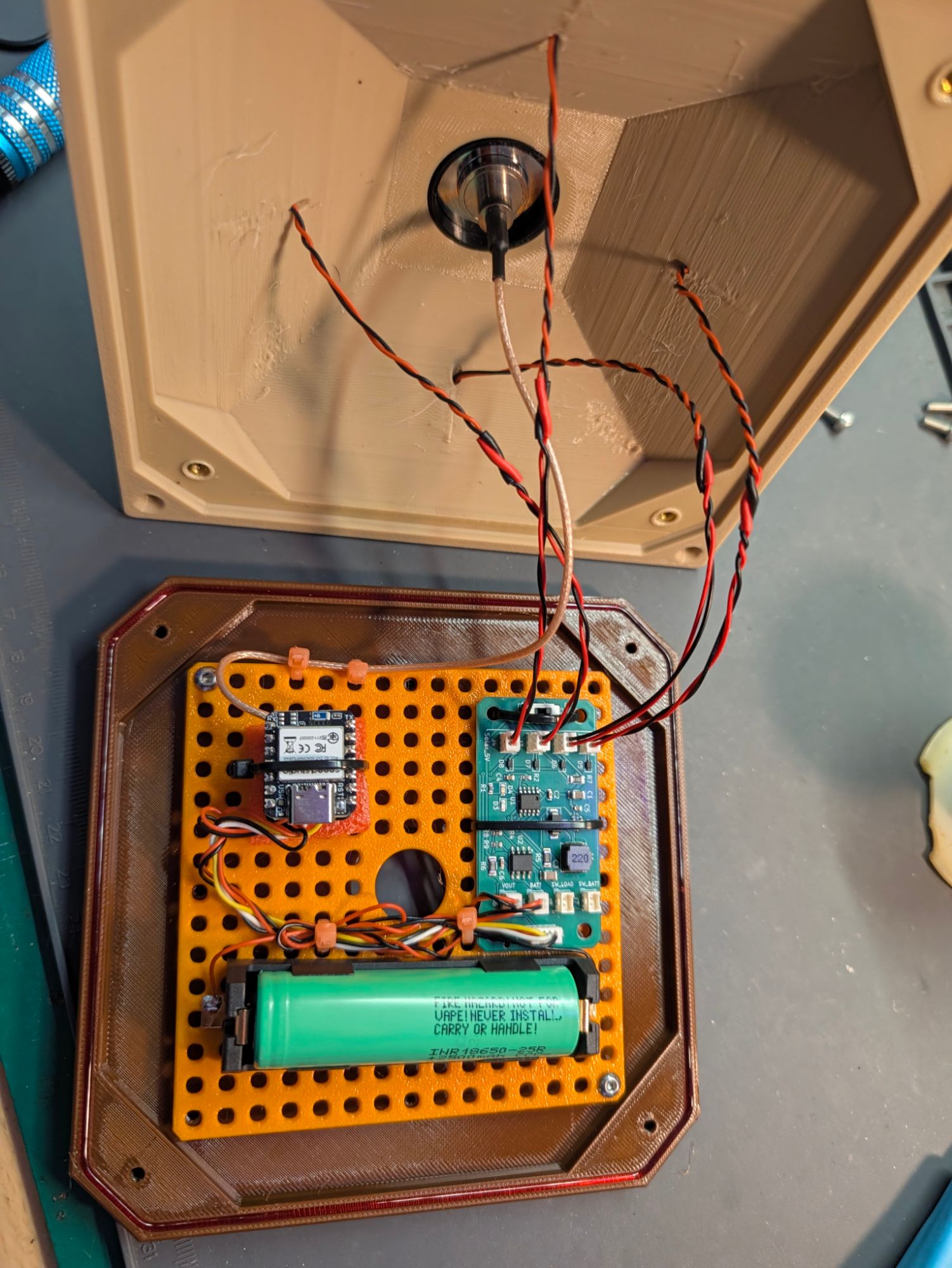
Status: the schematic is complete and passes ERC. The PCB (56.5 × 29 mm, 2mm corner chamfers, four M3 mounting holes, two layers) is placed and auto-routed with a clean DRC, but hasn't had a manual layout review. A first board has been wired up and tested with a XIAO + Wio-SX1262 on a custom Meshtastic build, and everything seems to work as expected so far, including the I2C sensor. A sunlight test in a real solar node is under way, with the expected voltage and charge current so far. See Testing.
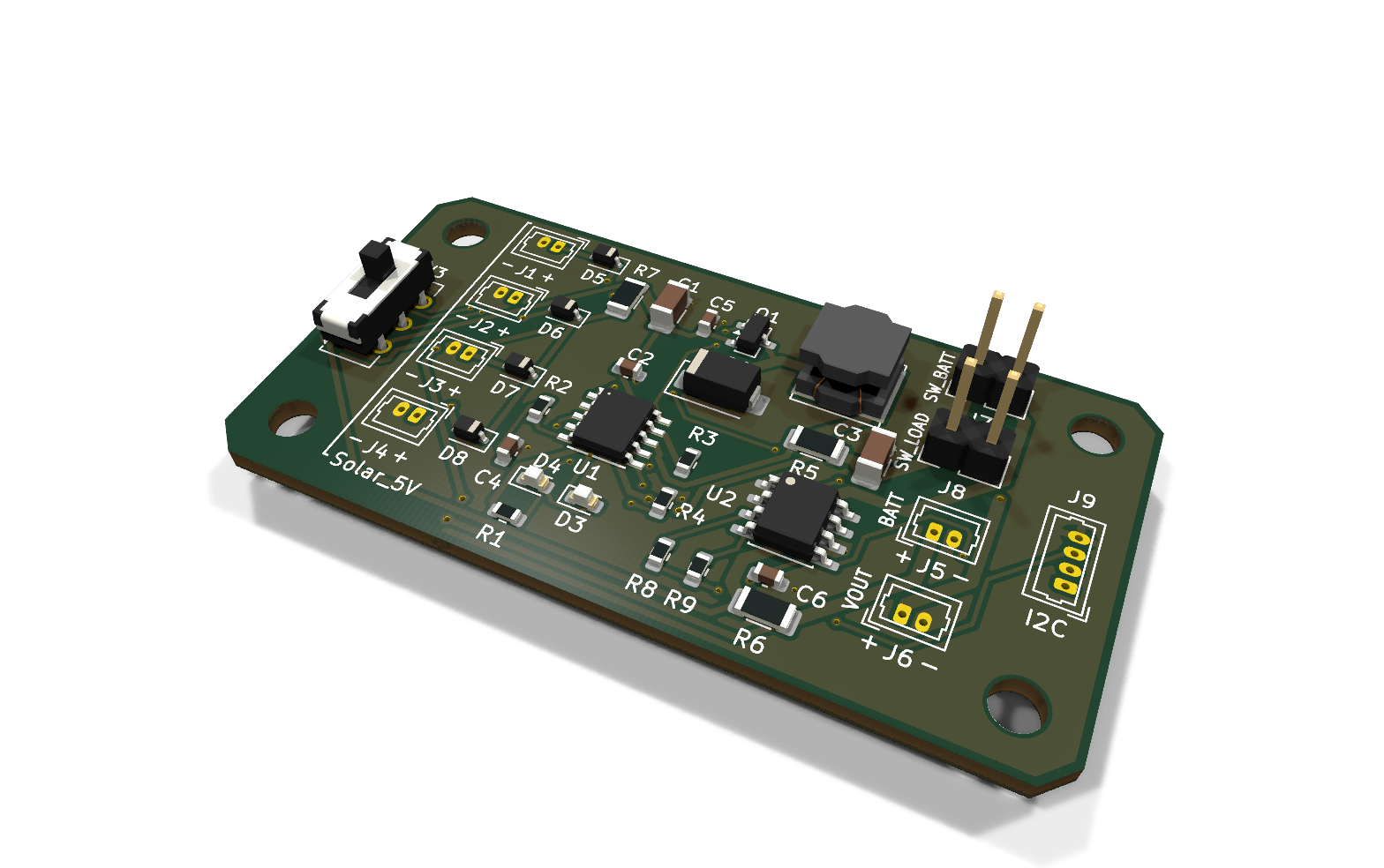
This controller is meant for solar mesh nodes like the SNAP v1.2: Solar Node Adaptable Platform. It simplifies their build in three ways:
I2C power sensors are supported natively by both Meshtastic and MeshCore. In most cases the node recognizes the INA219 automatically once it's connected.
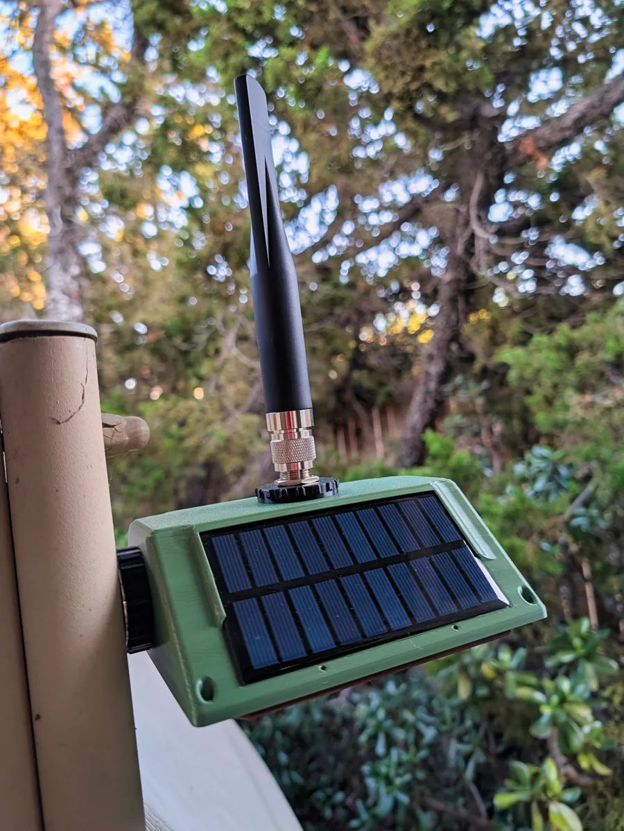
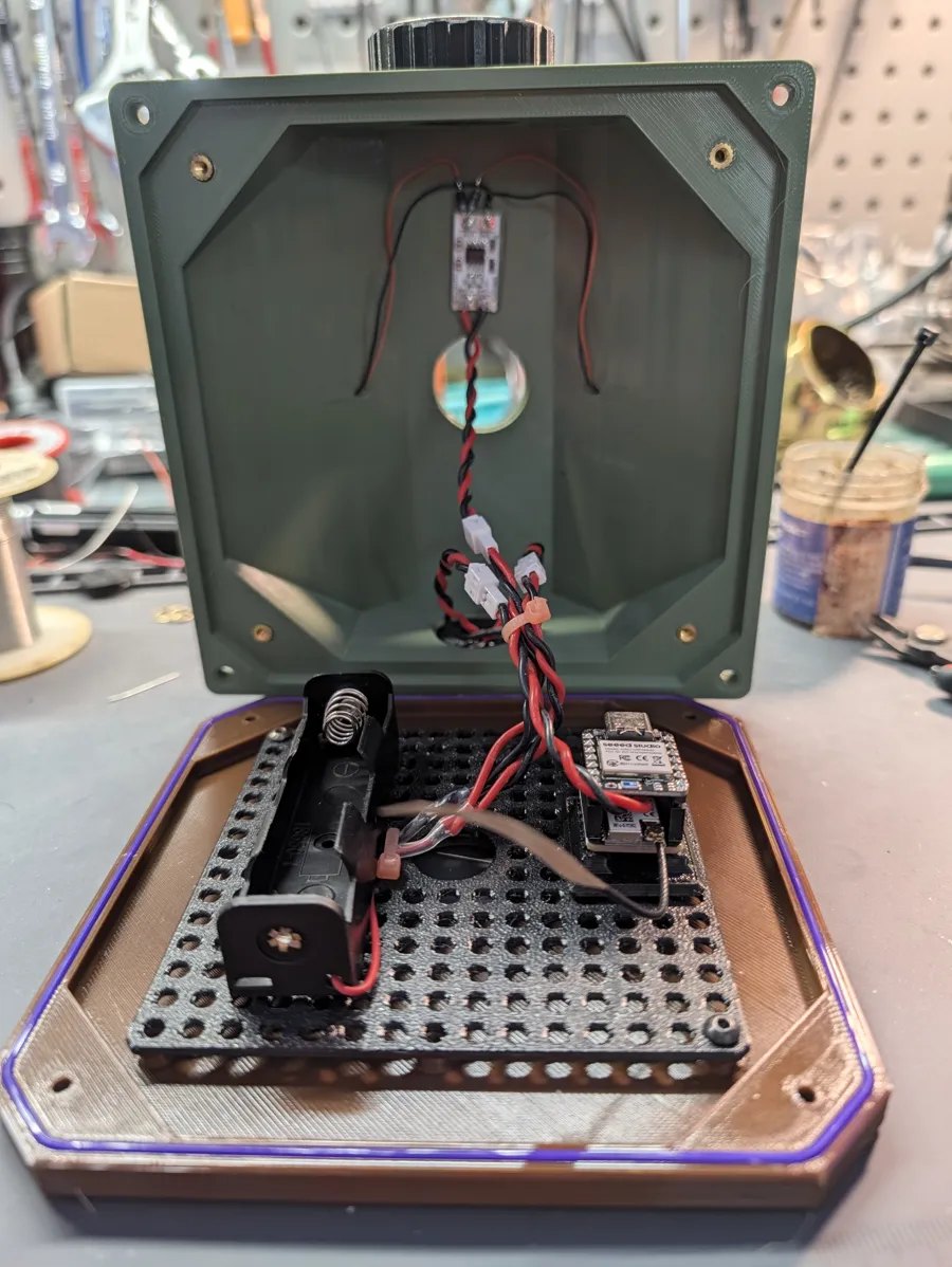
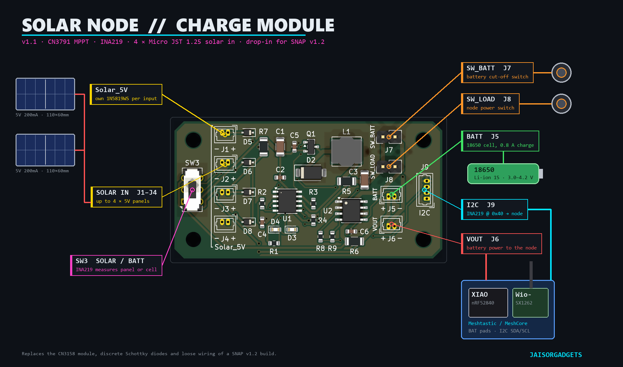
In the SNAP v1.2 example build, shown below, the board replaces several separately wired parts:
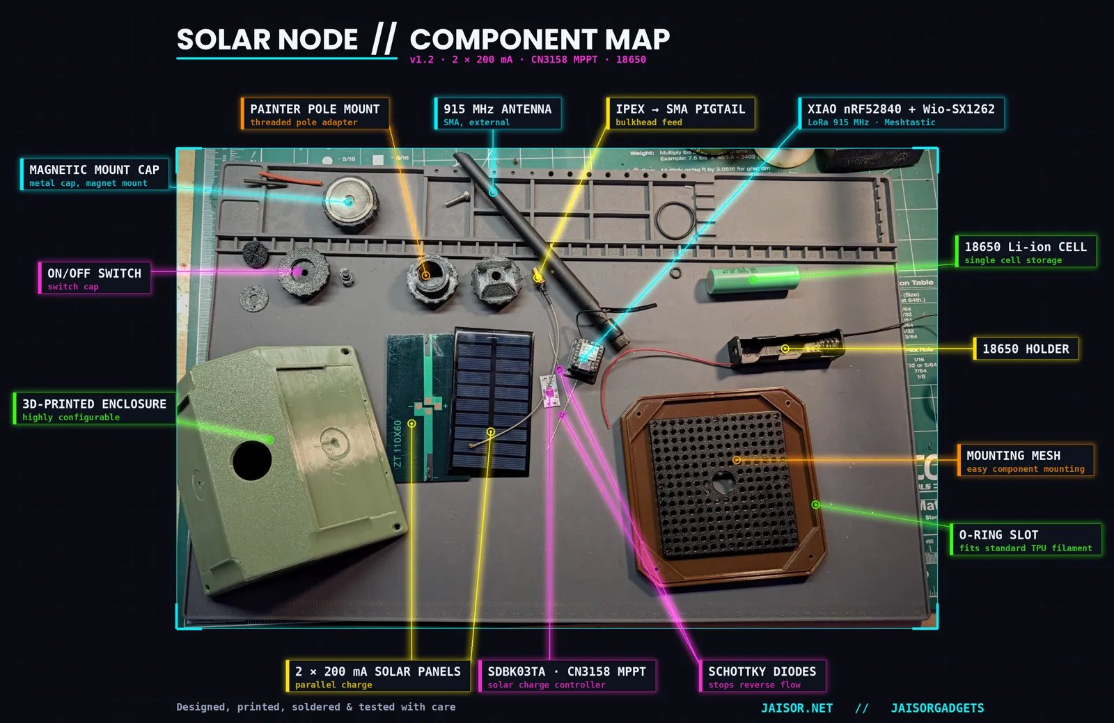
| Example build part | With this board |
|---|---|
| CN3158 MPPT module (SDBK03TA) | CN3791 MPPT buck charger, tuned for 5V panels (VIN held at 4.58V) and charging at 0.8A |
| One 1N5819 per panel, soldered inline | A 1N5819WS per input on the board, for up to four panels |
| Hand-soldered panel, battery and node wiring | Plug-in connectors for every connection: Micro JST 1.25, with 2.54mm pin headers for the switches |
| Latching on/off switch wired into the battery lead | Two switch connectors: SW_BATT cuts the battery, SW_LOAD cuts only the node |
| (none) | INA219 power monitor on I2C, switchable between the panels and the battery |
| Board connector | Connects to |
|---|---|
| J1, J2 (Solar_5V) | Two FellDen 5V 200mA 110×60mm panels, the ones SNAP v1.2 uses. J3 and J4 take up to two more |
| J5 (BATT) | An 18650 Li-ion cell (1S, 3.0–4.2V) in its holder |
| J8 (SW_LOAD) | The SNAP on/off switch cap's latching button. To cut the battery entirely, use J7 (SW_BATT) as well, or instead |
| J7 / J8 left unswitched | Both switch connectors are in series with the power path, so an unused one needs a 2.54mm jumper cap, or a wire bridging its pads on the back of the board. Otherwise the battery or the node stays disconnected |
| J6 (VOUT) | The XIAO nRF52840's BAT+ / BAT− pads, which is where SNAP powers it from the 18650 today |
| J9 (I2C) | XIAO 3V3 → VCC, D6 → SDA, D7 → SCL, GND → GND. These pins need a Meshtastic build with I2C on D6/D7 (see the table below) |
Set SW3 to BATT to see the battery's charge and discharge current, or to SOLAR to see what the panels deliver.
The XIAO's I2C pins depend on the firmware build. D4 and D5 can't be used with the Wio-SX1262, because the radio uses them.
| Firmware build | SDA | SCL | Status |
|---|---|---|---|
Meshtastic seeed_xiao_nrf52840_kit, custom build with I2C on D6/D7 | D6 | D7 | Tested on this board |
Meshtastic seeed_xiao_nrf52840_kit_i2c | D6 | D7 | From the firmware source, not tested |
Meshtastic seeed_xiao_nrf52840_kit, unmodified (D6/D7 are reserved for the GNSS module) | NFC1 pad (underside) | NFC2 pad (underside) | From the firmware source, not tested |
MeshCore Xiao_nrf52 | D7 | D6 | From the firmware source, not tested |
The INA219 uses address 0x40, which some other I2C sensors also use (for example the SHT21/HTU21D and HDC1080). If your node already has one of those, the two will clash.
In Meshtastic, enable power metrics in the telemetry settings so the readings are sent to the mesh.

The schematic follows the CN3791 datasheet's typical application circuit (Figure 1), with these changes:
| Item | Value | Why |
|---|---|---|
| Charge current | 0.8A (R5 = 0.15Ω) | ICH = 120mV / R5. Leaves margin on the 1.0A-rated connectors; use 0.24Ω for 0.5A with small cells. |
| MPPT setpoint | 4.58V at VIN (R3/R4 = 28.0k/10k) | VMPPT = 1.205V × (1 + R3/R4). The panels sit one diode drop higher (~4.9–5.0V), about the max-power voltage of a typical 5V panel. |
| Blocking diode D1 | omitted | The input diodes already stop the battery feeding back into the panels. Leaving D1 out saves ~0.4V of headroom; the trade-off is ~21µA of battery drain in the dark. |
| Inductor | 22µH, Bourns SRN6045TA | Meets the datasheet's L > 5 × (VCC − VBAT) µH, with ~0.2A ripple. |
| Input diodes | 1N5819WS, SOD-323 (40V/1A) | The panels peak at ~200–300mA each, so the SMD part has plenty of margin and saves ~12mm of board width over DO-41. |
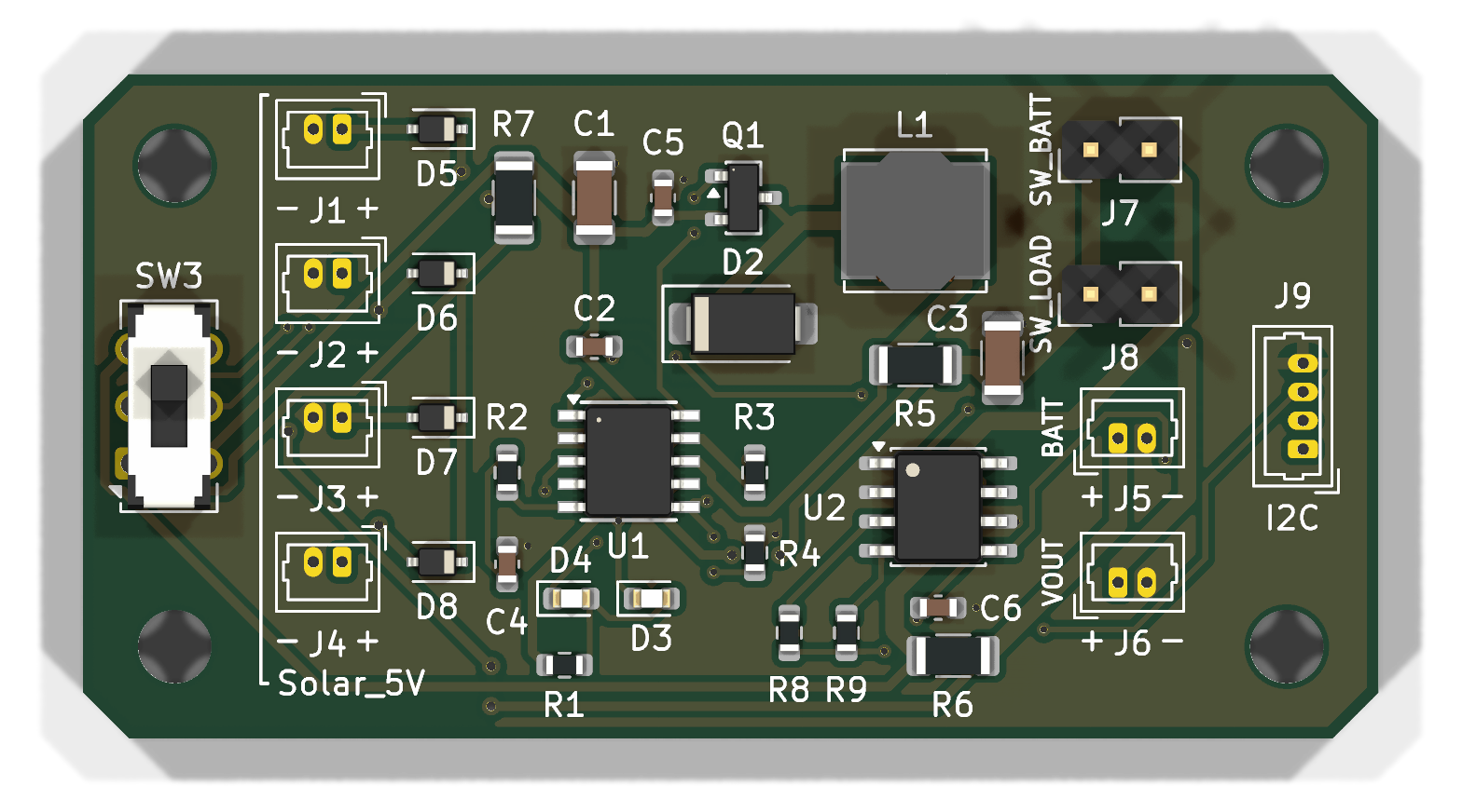
| Area | Parts |
|---|---|
| Left end | M3 mounting holes H1/H3 in the corners, with the SOLAR/BATT selector SW3 between them |
| Left column | Solar inputs J1–J4, each with its 1N5819WS (D5–D8) |
| Top middle | Buck power stage in current-flow order: R7, C1/C5, Q1, D2, L1, R5, C3 |
| Middle | CN3791 (U1) with its support parts and status LEDs |
| Right middle | INA219 (U2), I2C pull-ups, battery shunt R6 |
| Right column | SW_BATT/SW_LOAD switch leads (J7/J8), battery J5, VOUT J6 |
| Right end | M3 mounting holes H2/H4 in the corners, with the 4-pin I2C connector J9 between them |
Every reference label sits next to its own part, clear of pads, other parts and the edge (DRC reports no silkscreen issues). The holes are plain non-plated 3.2mm M3 holes, 4mm in from each edge.
Silkscreen labels:
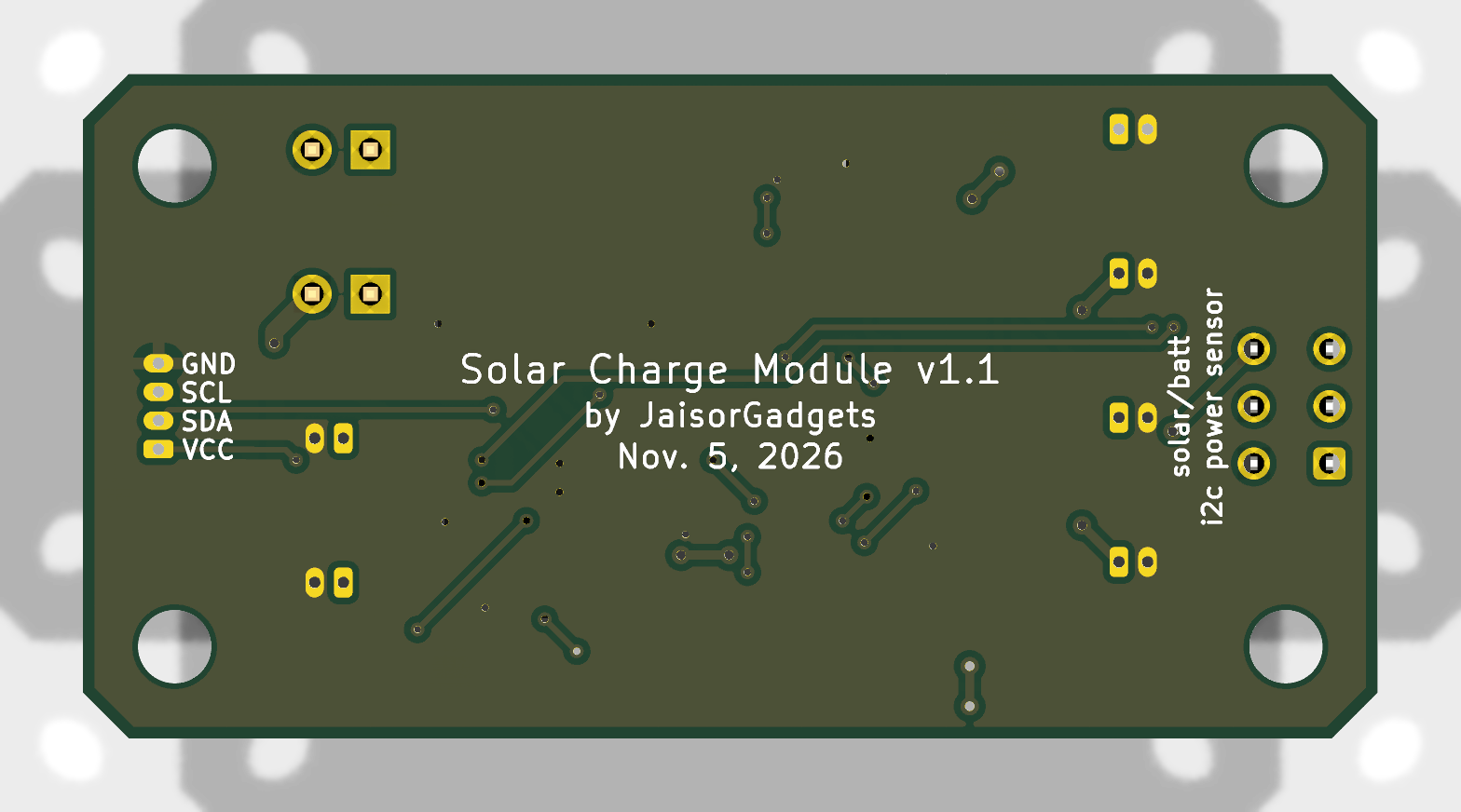
SW_BATT (J7), SW_LOAD (J8), BATT (J5) and VOUT (J6).Solar_5V label, with a bracket along the four solar inputs (J1–J4).- and + under the solar, battery and VOUT connectors (J1–J6), on the side of the matching pin.I2C under J9 on the front. The pin names (VCC, SDA, SCL, GND) are printed beside its pads on the back, since there's no room between the pads and the connectors on the front.solar/batt / i2c power sensor beside SW3 on the back, with "solar" at the end of the switch that has the PV pins and "batt" at the end with the battery pins.Routing (by tools/route-pcb.py):
This is auto-routing, so review it before ordering, especially the buck converter's switching loop (C1 → Q1 → D2, which currently returns through the ground plane) and the few bottom-layer tracks that cut the plane.
Still to do: a manual layout review before ordering (see Fabrication).
| Ref | Connector | Pin 1 | Pin 2 | Notes |
|---|---|---|---|---|
| J1–J4 | Micro JST 1.25, 2-pin | Panel + | GND | 5V solar panels, any combination of 1–4 |
| J5 | Micro JST 1.25, 2-pin | Battery + | GND | 1S Li-ion/LiPo, 4.2V |
| J6 | Micro JST 1.25, 2-pin | VOUT | GND | Battery voltage out to the powered module, through SW_LOAD |
| J7 | 2.54mm pin header, 2-pin | VBAT (charger) | BATT+ (battery) | SW_BATT: panel-mount SPST switch, rated ≥1A or the module's peak current |
| J8 | 2.54mm pin header, 2-pin | VBAT | VOUT | SW_LOAD: panel-mount SPST switch, same rating |
| J9 | Micro JST 1.25, 4-pin | VCC (3.3–5V) | SDA | Pin 3 = SCL, pin 4 = GND. VCC comes from the MCU and powers the INA219. |
J1–J6 and J9 are Micro JST 1.25 (Molex PicoBlade-compatible) vertical headers, Molex 53047-0210 (2-pin) and 53047-0410 (4-pin). They mate with standard female cable housings (Molex 51021). J7 and J8 are standard 2.54mm vertical pin headers, which take a 2.54mm female housing or a jumper cap. Notes:
+ (pin 1 on J5) before connecting.+ on J1–J6. J1–J4 are rotated 180° from J5 and J6, so the marks read - J1 + on the solar inputs and + J5 - on the right-hand connectors.Operating note: if SW_BATT is off while the panels are in sun, the charger sees no battery and VBAT pulses around 4.2V. Keep SW_LOAD off in that state.
| SW3 position | Shunt | Current | Bus voltage |
|---|---|---|---|
| SOLAR | R7, between the PV bus and VIN | Panel current, always ≥ 0 | VIN (panel voltage minus the diode drop) |
| BATT | R6, between BATT+ and the cell | Positive while charging, negative while discharging | Cell voltage, readable even with SW_BATT off |
The MCU can't sense SW3's position. Firmware has to know which position is set, or infer it from the readings.
| Test | Setup | Status |
|---|---|---|
| First power-up | Board wired to a XIAO + Wio-SX1262, running Meshtastic built from seeed_xiao_nrf52840_kit with I2C on D6/D7 | Done. Everything seems to work as expected, including the INA219 over I2C |
| INA219 battery current | Same setup, battery at about 4V | Done. Discharging: about −12 to −15mA. Charging from the XIAO's USB: +100mA |
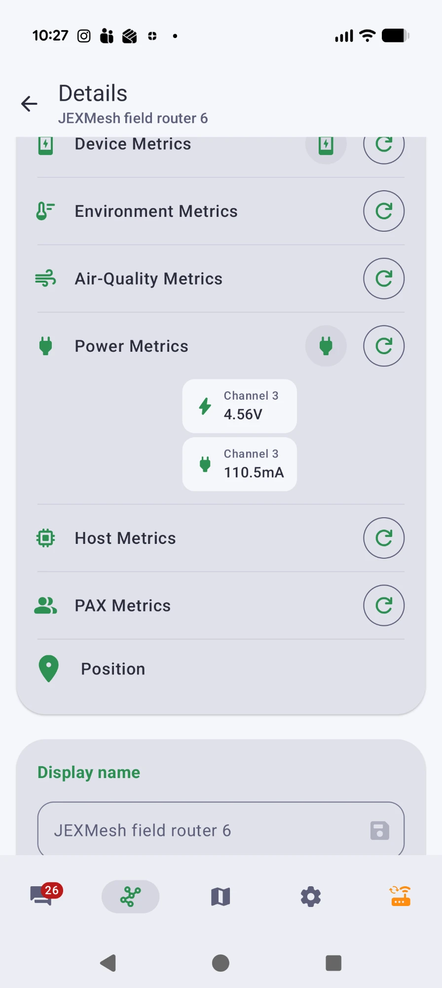
| Sunlight | Board wired into a real solar node with 4 × 60mA panels, with metrics tracked in Grafana dashboards | In progress. Voltage and charge current rose as expected when exposed to sunlight. One reading in the Meshtastic app: 4.56V, 110.5mA |
The signs match the expected convention: positive while charging, negative while discharging. The USB reading comes from the XIAO's own charger, so it doesn't test the CN3791. The sunlight reading is from SW3's SOLAR position: 4.56V is above a Li-ion cell's 4.2V and close to the 4.58V MPPT set point. It's a single reading, and longer-term results are still to come. These tests used a board with Micro JST 1.25 connectors on J7 and J8, so the pin-header version hasn't been built yet. In the sunlight test build, J7 and J8 are bridged with wire on the back of the board, so neither switch is fitted.
Download the package from the latest release. That release is v1.0, which has Micro JST 1.25 connectors on J7 and J8 and no polarity marks. The design in this repo is v1.1, still a work in progress, and it will be released with the next fabrication batch. The package is generated into output/fab/, which isn't tracked in git:
| File | Contents |
|---|---|
SolarChargeModule_v1.1_gerbers.zip | Upload this to the board house. 9 Gerber X2 layers (copper, mask, paste and silkscreen on both sides, plus the outline), a Gerber job file, plated and non-plated Excellon drill files, and drill maps |
FAB_NOTES.txt | Order settings: 2 layers, FR-4 1.6mm, 1oz copper, 56.5 × 29mm, 0.25mm/0.2mm minimum track/space, 0.3mm minimum drill, tented vias, four 3.2mm non-plated holes. Also assembly cautions |
SolarChargeModule_v1.1_BOM.csv | BOM in JLCPCB format (Comment, Designator, Footprint, LCSC Part #), plus a Manufacturer Part column for the specific parts |
SolarChargeModule_v1.1_CPL.csv | Pick-and-place file for top-side assembly, in the same coordinates as the Gerbers |
LCSC part numbers are only filled in where verified (D5–D8). Pick the rest in the assembler's part search, and check rotation and polarity in their preview. The PicoBlade headers, the J7 and J8 pin headers, and SW3 are through-hole parts.
Regenerating the package (after the board is final and DRC is clean):
OUT=output/fab
P=SolarNodeChargeController
kicad-cli pcb export gerbers --layers F.Cu,B.Cu,F.Paste,B.Paste,F.Silkscreen,B.Silkscreen,F.Mask,B.Mask,Edge.Cuts --subtract-soldermask --check-zones -o $OUT/gerbers $P.kicad_pcb
kicad-cli pcb export drill --format excellon --excellon-units mm --excellon-zeros-format decimal --drill-origin absolute --excellon-separate-th --generate-map --map-format gerberx2 -o $OUT/gerbers/ $P.kicad_pcb
kicad-cli pcb export pos --format csv --units mm --side both -o $OUT/pos-kicad.csv $P.kicad_pcb
kicad-cli sch export bom --fields 'Value,Reference,Footprint,${QUANTITY}' --labels 'Comment,Designator,Footprint,Qty' --group-by 'Value,Footprint' --ref-range-delimiter '' --exclude-dnp -o $OUT/bom-kicad.csv $P.kicad_sch
node tools/fab-package.js $OUTSolarNodeChargeController.kicad_pro / .kicad_sch / .kicad_pcb KiCad project
SolarNode.kicad_sym project symbol library (CN3791)
sym-lib-table
tools/
gen-schematic.js generates the schematic (Node)
place-pcb.py places footprints, labels, holes, outline (KiCad Python / pcbnew)
route-pcb.py routes tracks, GND stitching vias and pours (run after place-pcb.py)
make-diagram.py draws docs/images/wiring-diagram.png from the board render
fab-package.js JLCPCB-style BOM/CPL, fab notes and Gerber zip from the kicad-cli exports
docs/images/ images used in this README (snap/: photos from the SNAP v1.2 MakerWorld post)
CLAUDE.md design decisions and working notesThe schematic and the board layout are generated by scripts in tools/, and checked with kicad-cli ERC/DRC (including schematic parity). See CLAUDE.md for the full design rationale and workflow. Generated outputs (output/: BOM, reports, fab files) are not tracked.
The whole design can be rebuilt from the scripts. Run these from the repo root, with kicad-cli from KiCad 10:
# 1. Schematic (Node): rewrites the .kicad_sch, SolarNode.kicad_sym and sym-lib-table
node tools/gen-schematic.js
kicad-cli sch erc --format json --severity-all -o erc.json SolarNodeChargeController.kicad_sch
# 2. Netlist for the board scripts
kicad-cli sch export netlist --format kicadxml -o net.xml SolarNodeChargeController.kicad_sch
# 3. Board (KiCad's Python): placement + labels + holes + outline, then routing + GND pours (~5 min)
"C:/Program Files/KiCad/10.0/bin/python.exe" tools/place-pcb.py net.xml
"C:/Program Files/KiCad/10.0/bin/python.exe" tools/route-pcb.py
# 4. Check: expect 0 violations, 0 unconnected, 0 parity issues
kicad-cli pcb drc --schematic-parity --severity-all --format json -o drc.json SolarNodeChargeController.kicad_pcb
The scripts overwrite their output files. Once you edit the schematic or board in KiCad, stop regenerating that file (or port your edits into the scripts first).
Refreshing the images in docs/images/:
kicad-cli sch export svg -o docs/images SolarNodeChargeController.kicad_sch
kicad-cli pcb render --side top --width 1600 --height 900 --quality high --zoom 1.6 -o docs/images/pcb-top.png SolarNodeChargeController.kicad_pcb
kicad-cli pcb render --side bottom --width 1600 --height 900 --quality high --zoom 1.6 -o docs/images/pcb-bottom.png SolarNodeChargeController.kicad_pcb
kicad-cli pcb render --width 1600 --height 1000 --quality high --perspective --rotate "-40,0,-25" -o docs/images/pcb-iso.png SolarNodeChargeController.kicad_pcb
(The schematic export is named SolarNodeChargeController.svg; rename it to schematic.svg.)
After refreshing pcb-top.png, redraw the wiring diagram with KiCad's Python, which includes Pillow and NumPy:
"C:/Program Files/KiCad/10.0/bin/python.exe" tools/make-diagram.py| Qty | Value | Footprint | References |
|---|---|---|---|
| 4 | 1N5819WS | Diode_SMD:D_SOD-323 | D5, D6, D7, D8 |
| 4 | M3 | MountingHole:MountingHole_3.2mm_M3 | H1, H2, H3, H4 |
| 4 | Solar_5V | Connector_Molex:Molex_PicoBlade_53047-0210_1x02_P1.25mm_Vertical | J1, J2, J3, J4 |
| 2 | 0.1R 1% | Resistor_SMD:R_1206_3216Metric | R6, R7 |
| 2 | 100nF | Capacitor_SMD:C_0603_1608Metric | C2, C6 |
| 2 | 10k | Resistor_SMD:R_0603_1608Metric | R8, R9 |
| 1 | 0.15R 1% | Resistor_SMD:R_1206_3216Metric | R5 |
| 1 | 100nF/25V | Capacitor_SMD:C_0603_1608Metric | C5 |
| 1 | 10k 1% | Resistor_SMD:R_0603_1608Metric | R4 |
| 1 | 10uF/25V | Capacitor_SMD:C_1206_3216Metric | C1 |
| 1 | 120R | Resistor_SMD:R_0603_1608Metric | R2 |
| 1 | 1k | Resistor_SMD:R_0603_1608Metric | R1 |
| 1 | 220nF | Capacitor_SMD:C_0603_1608Metric | C4 |
| 1 | 22uF/10V | Capacitor_SMD:C_1206_3216Metric | C3 |
| 1 | 22uH | Inductor_SMD:L_Bourns_SRN6045TA | L1 |
| 1 | 28.0k 1% | Resistor_SMD:R_0603_1608Metric | R3 |
| 1 | AO3401A | Package_TO_SOT_SMD:SOT-23 | Q1 |
| 1 | CN3791 | Package_SO:SSOP-10_3.9x4.9mm_P1.00mm | U1 |
| 1 | GREEN | LED_SMD:LED_0603_1608Metric | D3 |
| 1 | I2C_MCU | Connector_Molex:Molex_PicoBlade_53047-0410_1x04_P1.25mm_Vertical | J9 |
| 1 | INA219AID | Package_SO:SOIC-8_3.9x4.9mm_P1.27mm | U2 |
| 1 | LiPo_1S_4.2V | Connector_Molex:Molex_PicoBlade_53047-0210_1x02_P1.25mm_Vertical | J5 |
| 1 | RED | LED_SMD:LED_0603_1608Metric | D4 |
| 1 | SOLAR / BATT | Button_Switch_THT:SW_CK_JS202011CQN_DPDT_Straight | SW3 |
| 1 | SS34 | Diode_SMD:D_SMA | D2 |
| 1 | SW_BATT | Connector_PinHeader_2.54mm:PinHeader_1x02_P2.54mm_Vertical | J7 |
| 1 | SW_LOAD | Connector_PinHeader_2.54mm:PinHeader_1x02_P2.54mm_Vertical | J8 |
| 1 | VOUT | Connector_Molex:Molex_PicoBlade_53047-0210_1x02_P1.25mm_Vertical | J6 |
It measures 56.5 × 29 mm and has 2 copper layers, 1.6 mm thick.
40 parts, built around the INA219AID, CN3791, 1N5819WS and AO3401A. The full list of its parts is on this page, with links to each part's symbol and footprint where PCBKit's library has them.
From the jaisor/SolarNodeChargeController repository on GitHub, at the commit this page was made from: the board is SolarNodeChargeController.kicad_pcb and its schematic SolarNodeChargeController.kicad_sch. PCBKit opens the board in the browser, with nothing to install.
Its repository states no licence, so its author keeps all rights: ask jaisor before reusing the design.
LEAT-EDGE/ambient-pcb-audiopower
Audio capture and energy management daughterboard PCB for the Ambient project.

3351666087/solar-vest
Self-powered solar-harvesting wearable ECG vest: PCBs, 3D-printed enclosures, vest patterns, simulation and an interactive 3D explorer

sercami97/EstacionMeteorologica
Open source proyect for low cost weather station


gargsrishtii/TankSync-tx
Solar-powered transmitter PCB for TankSync wireless tank monitoring system — ESP32-C3 + LoRa + ultrasonic sensor, KiCad 10.0

jadenrhee/wigglecam-controller
RP2040 co-processor board for a 4-lens wigglegram camera: constant-current flash, controls, battery telemetry, Pi 5 I2C interface. 4-layer, DRC-clean, fab-ready.

Abhi90808/Solar-MPPT-Charger-CN3791-
Solar Li-ion battery charger PCB using the CN3791 MPPT IC, optimized for single-cell charging from small solar panels with automatic maximum power point tracking.

Hidayatur-rahman/Solar-Water-Level-Monitor-ESP8266-ESPHome-
A solar-powered water tank level monitoring system built around the ESP8266 (ESP-12E), designed in KiCad and running on ESPHome