2 layers50 × 66 mm

 jacdac/jacdac-ddk2
Jacdac Device Development Kit
Slider is an open-source printed circuit board by jacdac, from the jacdac/jacdac-ddk repository on GitHub, published under the CC-BY-4.0 licence. It is a 2-layer board of 15 × 65.7 mm with 26 parts on 26 nets, routed with 238 tracks and 19 vias.
It is built around the XC6206P332MR, RCLAMP0521P-N and BAT54S. Its parts include 6 diodes, 4 capacitors, 4 resistors, 3 connectors and 2 ICs. It belongs with the STM32 boards of this library.


This is an example / reference Jacdac module for a slider potentiometer built in KiCad, an open-source PCB design suite.
| Schematic | Board |
|---|---|
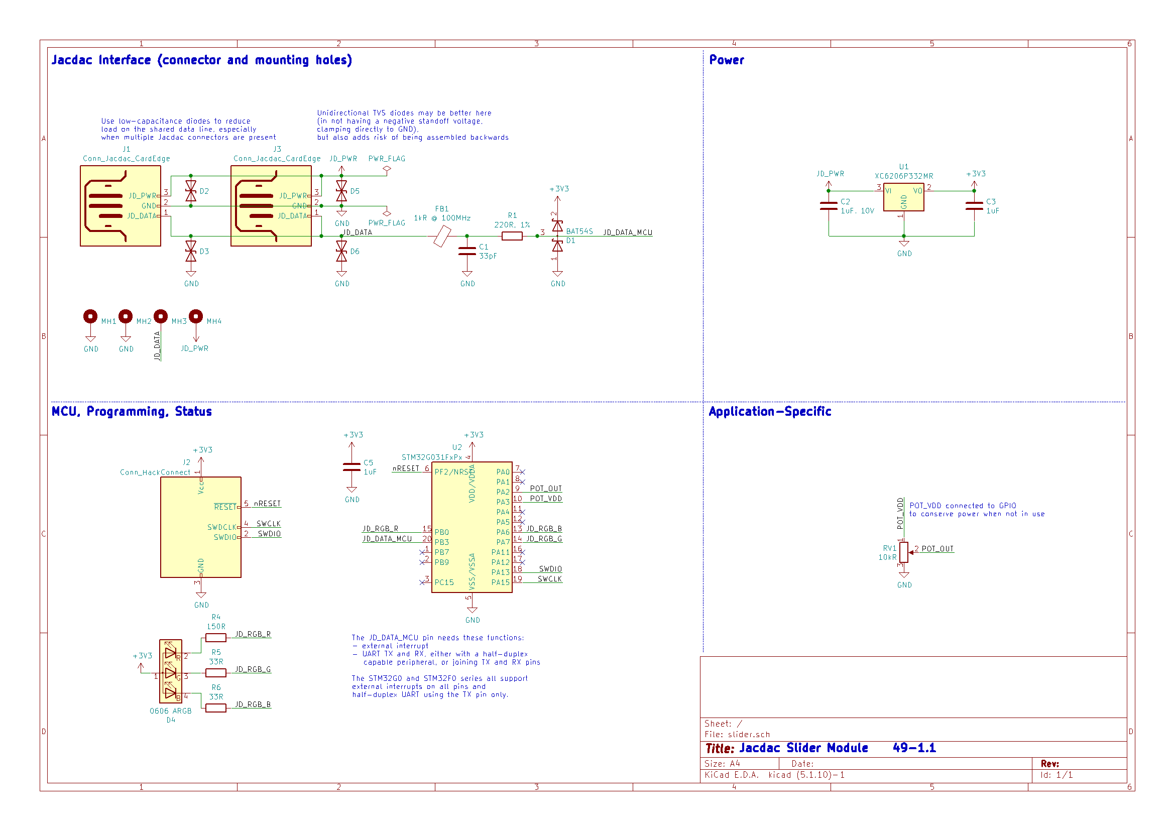 | Front side 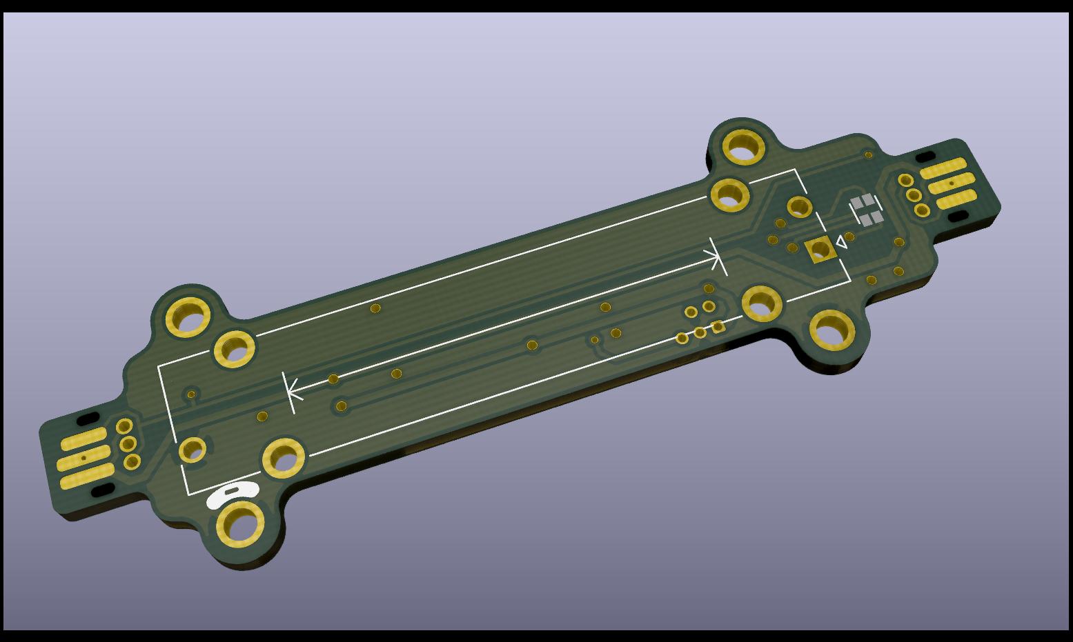 Back side 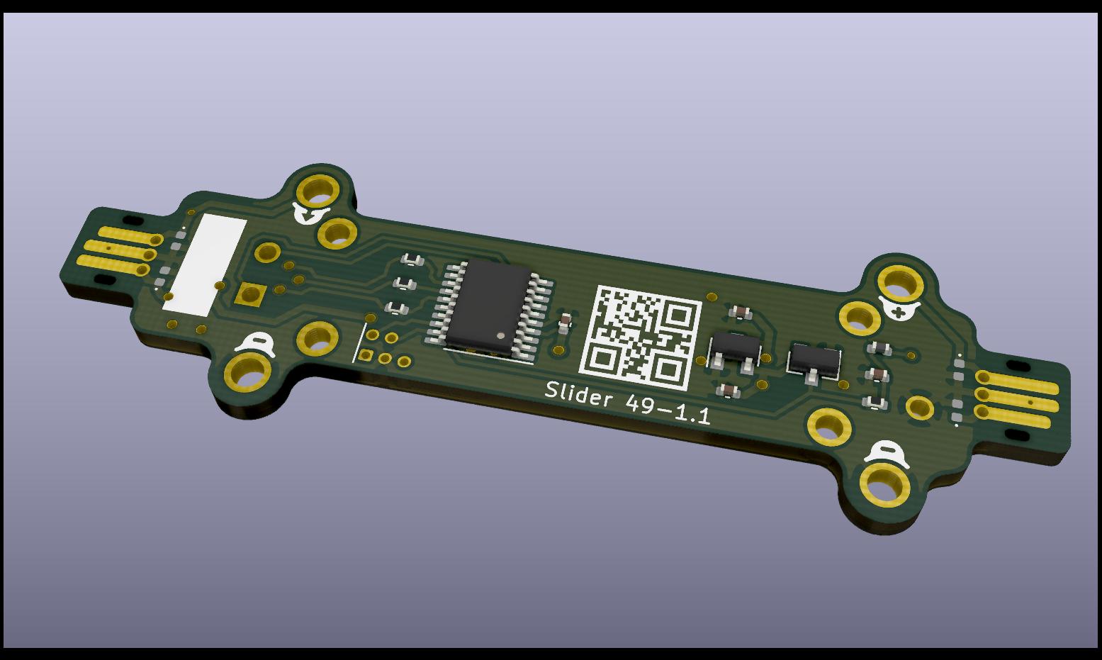 |
This KiCad project uses local (per-project, relative path) references to the Jacdac symbol and footprint libraries that are included in this repository.
This also includes a project-specific slider.pretty footprint library containing the module QR code,
as generated by the Jacdac Silk QR Code generator.
Fabrication data (gerbers, pick-and-place) is included in the fab-1.1 folder.
We fabricated our prototype run for this board with JLCPCB, which offers low-volume board fabrication and single-sided assembly services. Below are notes for how we generated fabrication data.
Gerbers can be generated with the typical KiCad flow.
In the schematic, we added a LCSC field to all components, containing the JLCPCB part numbers.
To generate the pick-and-place parts: in the schematic editor, go to Tools menu > Generate Bill of Materials..., run bom2grouped_csv, which produces a slider.csv in the project directory.
This should have an LCSC column with the JLC part numbers.
Rename columns as follows:
Reference -> DesignatorsLCSC -> LCSC Part #Value -> CommentNote: this was built against an older JLCPCB sample BoM file which used the column name LCSC Part #, instead of the JLCPCB Part # used in a newer sample BoM.
In the layout editor, go to File menu > Fabrication Outputs > Footprint Position (.pos) File...
Since JLC does one layer only, select "Separate files for front and back".
This creates a slider-bottom-pos.csv (and top file that can be discarded) in the output directory.
Rename columns as follows:
Ref -> DesignatorPosX -> Mid XPosY -> Mid YSide -> LayerOptionally, correct rotations on parts. While we've sent in fabrication data with obviously wrong rotations (eg, TSSOP-20 oriented 90 degree off) and didn't get obviously wrong PCBs back, you can correct the rotations using a spreadsheet tool like Excel:
Rot to something different, eg KiCadRot.RotCorrection column or something, to be manually set for each part. Positive rotation is clockwise (unmirrored view, at least on the bottom layer).Rotation column, set to the formula of the KiCadRot cell plus the RotCorrection cell. This is the column containing the actual fabrication data.In the PCB options, choose:
In the SMT Assembly options, choose:
slider.csv file (schematic BoM)slider-bottom-pos.csv file (layout footprint position)Stencils:
| Qty | Value | Footprint | References |
|---|---|---|---|
| 4 | RCLAMP0521P-N | Diode_SMD:D_0402_1005Metric | D2, D3, D5, D6 |
| 2 | 1uF | Capacitor_SMD:C_0402_1005Metric | C3, C5 |
| 2 | 33R | Resistor_SMD:R_0402_1005Metric | R5, R6 |
| 2 | Conn_Jacdac_CardEdge | Connector_Jacdac:JD-PEC-02_Prerouted | J1, J3 |
| 1 | slider:QrCode | ||
| 1 | 0606 ARGB | LED_SMD:LED_LiteOn_LTST-C19HE1WT | D4 |
| 1 | 10kR | Potentiometer_THT:Potentiometer_Bourns_PTA3043_Single_Slide | RV1 |
| 1 | 150R | Resistor_SMD:R_0402_1005Metric | R4 |
| 1 | 1kR @ 100MHz | Inductor_SMD:L_0402_1005Metric | FB1 |
| 1 | 1uF, 10V | Capacitor_SMD:C_0402_1005Metric | C2 |
| 1 | 220R, 1% | Resistor_SMD:R_0402_1005Metric | R1 |
| 1 | 33pF | Capacitor_SMD:C_0402_1005Metric | C1 |
| 1 | BAT54S | Package_TO_SOT_SMD:SOT-23 | D1 |
| 1 | Conn_HackConnect | Connector_Jacdac:HackConnect_P1.27mm | J2 |
| 1 | MountingHole_Pad | Connector_Jacdac:JD_MountingHole_Power | MH4 |
| 1 | MountingHole_Pad | Connector_Jacdac:JD_MountingHole_Data | MH3 |
| 1 | MountingHole_Pad | Connector_Jacdac:JD_MountingHole_Ground | MH2 |
| 1 | MountingHole_Pad | Connector_Jacdac:JD_MountingHole_Pin1 | MH1 |
| 1 | STM32G031FxPx | Package_SO:TSSOP-20_4.4x6.5mm_P0.65mm | U2 |
| 1 | XC6206P332MR | Package_TO_SOT_SMD:SOT-23 | U1 |
It measures 15 × 65.7 mm and has 2 copper layers, 1.6 mm thick.
26 parts, built around the XC6206P332MR, RCLAMP0521P-N and BAT54S. The full list of its parts is on this page, with links to each part's symbol and footprint where PCBKit's library has them.
From the jacdac/jacdac-ddk repository on GitHub, at the commit this page was made from: the board is electronics/deprecated_form_factor/kicad_deprecated/reference-designs/slider/slider.kicad_pcb. PCBKit opens the board in the browser, with nothing to install.
Its repository publishes it under the CC-BY-4.0 licence: you may reuse it on that licence's terms (keep the author's notice, and for a copyleft licence share your changes alike).

MartinVerges/womolin-waterlevel
DIY project to build a smart fuel sensor for RVs or in other projects. It is based on air pressure and is able to measure fresh water as well as grey and black water levels with high precision.


harry10086/InkWord_ESP32
An ESP32 and E-paper based low-power English vocabulary learning device.一个基于 ESP32 和墨水屏的低功耗英语单词学习设备。


hatlabs/HALMET-hardware
Hat Labs Marine Engine & Tank interface hardware design files