6 layers148 × 121 mm

 itsTasos/RAPS-5
Dual-input power module with independent LiPo protection, buck conversion and ideal-diode OR-ing.
RAPS-5 V1 is an open-source printed circuit board by itsTasos, from the itsTasos/RAPS-5 repository on GitHub. It is a 4-layer board of 50 × 40 mm with 96 parts on 45 nets, routed with 1,653 tracks and 204 vias.
It is built around the LTC4412ES6#TRPBF, TPS54561DPRR and TPS3808G01DBVR-TP, with the 2N7002-7-F-ES, XAL8080-103MED and BZT52H-C12 among its other parts. Its parts include 28 capacitors, 25 resistors, 9 diodes, 7 transistors and 5 ICs. It belongs with the power boards of this library.


Redundant Avionics Power Supervisor
A compact, dual-input power module for experimental UAV and robotics systems.
KiCad project · Schematic PDF · Bill of materials · Design notes · Bench validation
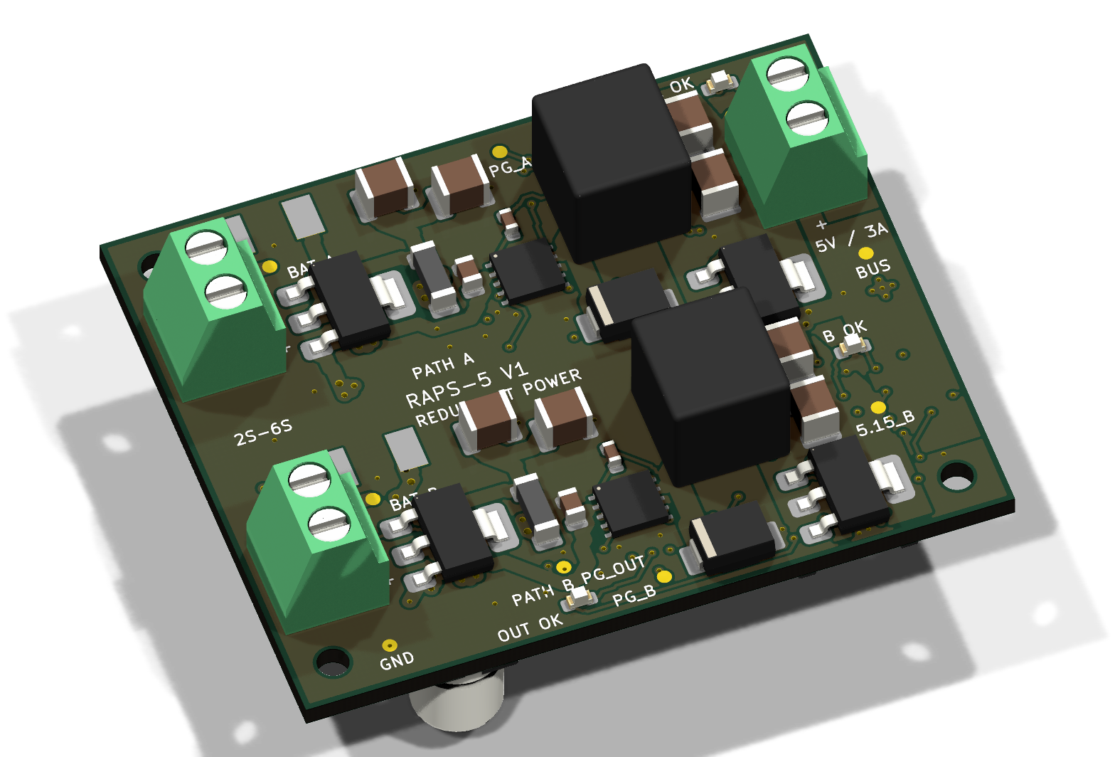
Prototype status — Schematic, PCB and fabrication exports are included. ERC, DRC and schematic-to-PCB parity checks pass under the saved project settings. 3 A continuous output is a design target; physical bench validation is pending.
RAPS-5 brings two independently protected LiPo inputs onto a common avionics power bus. Each path has its own fuse, reverse-polarity protection, transient suppression, input filtering and buck converter. Independent ideal-diode controllers combine the regulated outputs while blocking backfeed into an inactive path.
The result is a 50 × 40 mm, four-layer PCB with clearly labeled connectors, three voltage-status LEDs and accessible test points.
| At a glance | Design |
|---|---|
| Battery inputs | Two 2S–6S LiPo inputs; up to 25.2 V normal input |
| Local regulated outputs | Path A: 5.200 V · Path B: 5.152 V nominal |
| Continuous output | 3 A design target from either path |
| Buck converters | Two TPS54561DPRR devices, approximately 400 kHz |
| Output combining | Two LTC4412 controllers with external P-channel MOSFETs |
| PCB | 50 × 40 mm · 4 layers · 1.6 mm FR-4 · ENIG |
| Copper | 2 oz outer layers / 1 oz inner layers |
| Monitoring | PATH A OK · PATH B OK · OUTPUT OK |
| Design tool | KiCad 10; verified with 10.0.5 |
flowchart LR
    A["BAT A<br/>2S–6S LiPo"] --> PA["5 A fuse<br/>Reverse PMOS · TVS · Filter"]
    PA --> BA["TPS54561 buck<br/>5.200 V nominal"]
    BA --> OA["LTC4412 + PMOS<br/>Ideal-diode stage"]
    B["BAT B<br/>2S–6S LiPo"] --> PB["5 A fuse<br/>Reverse PMOS · TVS · Filter"]
    PB --> BB["TPS54561 buck<br/>5.152 V nominal"]
    BB --> OB["LTC4412 + PMOS<br/>Ideal-diode stage"]
    OA --> BUS["Common 5V_BUS<br/>Bulk + ceramic capacitors"]
    OB --> BUS
    BUS --> OUT["J3<br/>Avionics output"]
    BUS -.-> MON["TPS3808<br/>Output supervision"]
    style A fill:#123e35,stroke:#58ce9e,color:#fff
    style BA fill:#123e35,stroke:#58ce9e,color:#fff
    style B fill:#15354a,stroke:#79c5f4,color:#fff
    style BB fill:#15354a,stroke:#79c5f4,color:#fff
    style BUS fill:#203b43,stroke:#96dfcf,color:#fff
The positive power paths remain separate until OR-ing. Ground is shared; the inputs are not galvanically isolated. Each path is intended to support the full load on its own. The small voltage offset nominally favors A, but does not guarantee source priority or equal current sharing.
The 5.200 V and 5.152 V figures are converter setpoints before the OR-ing MOSFETs. Loaded BUS voltage is lower because of MOSFET and copper losses; approximately 5.1 V at 3 A is an estimate to verify on the bench.
| Top — power stages and connectors | Bottom — controls and bulk capacitance |
|---|---|
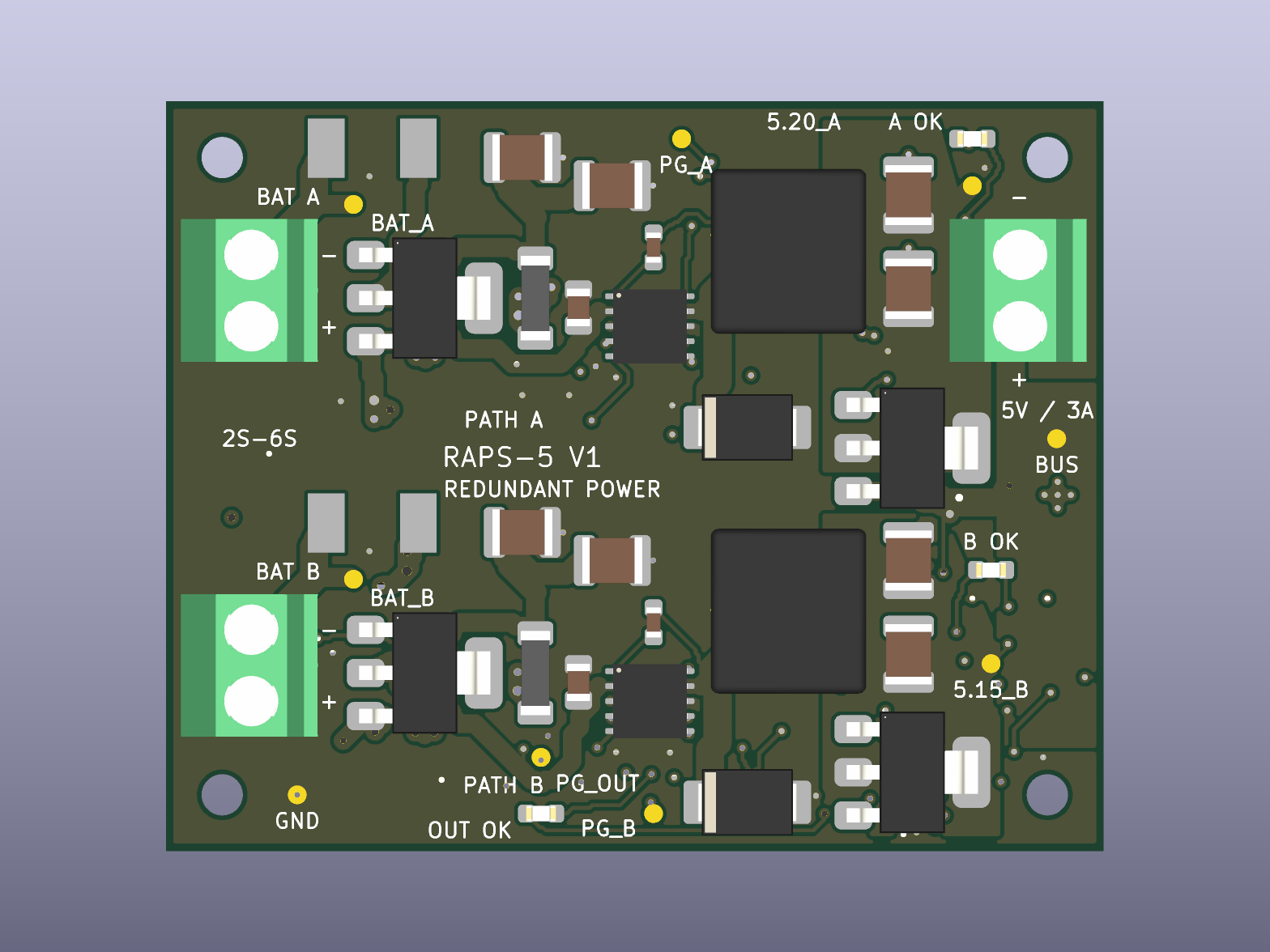 | 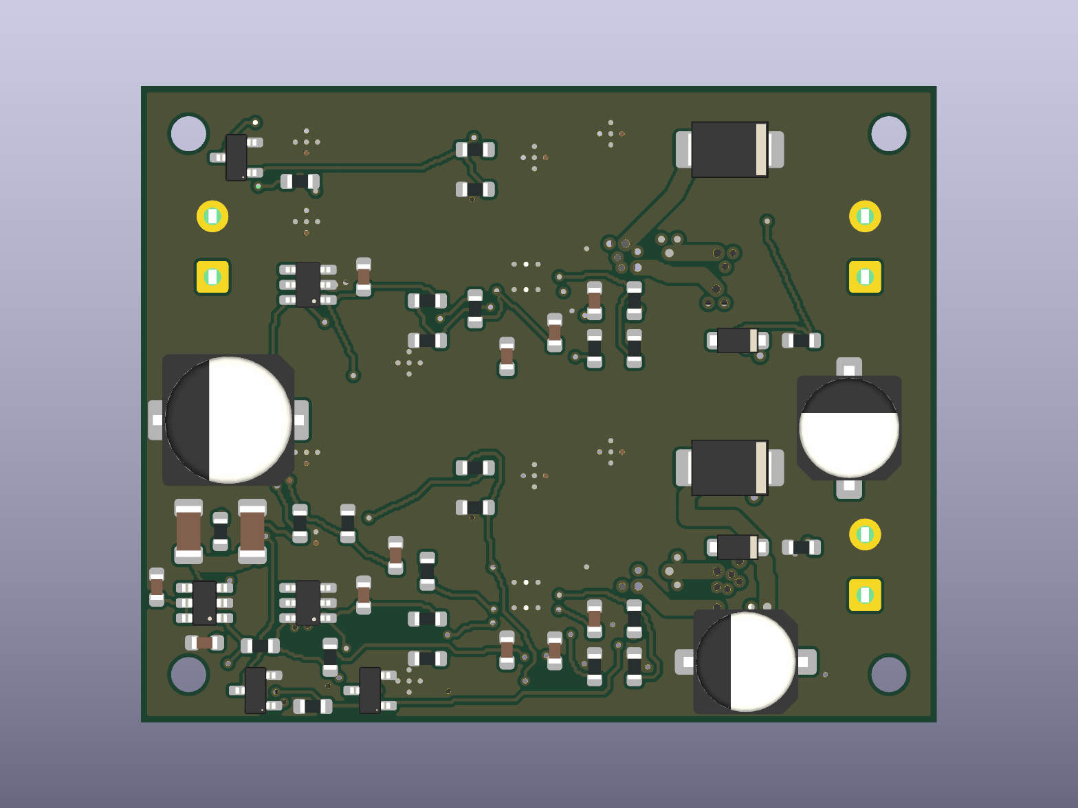 |
Images are CAD renders. Some components do not have 3D models; these are not photographs of an assembled or tested board.
| Connector | Function | Pin 1 | Pin 2 |
|---|---|---|---|
| J1 | Battery A input | BAT_A positive | GND |
| J2 | Battery B input | BAT_B positive | GND |
| J3 | Avionics output | 5V_BUS positive | GND |
All three use 3.81 mm, two-pin Phoenix terminal-block footprints. PATH A OK and PATH B OK indicate converter power-good status; OUTPUT OK indicates the supervised BUS voltage. LEDs do not indicate which source is carrying current. Power-good test points have local pullups; check voltage compatibility with external logic.
hardware/RAPS-5_V1.kicad_pro in KiCad 10.Project-local symbols and footprints are included under hardware/libraries/. The library tables use ${KIPRJMOD}, so no machine-specific library paths are required. No generator or autorouter script is needed to open or edit the delivered design.
hardware/                 Native KiCad project, four schematic sheets and PCB
  libraries/              Project-local symbols and footprints
docs/
  DESIGN.md               Circuit behavior, component choices and limits
  drawings/               Schematic, assembly and copper PDFs
  images/                 README artwork and native 3D renders
manufacturing/
  BOM.csv                 Component values, footprints and key part numbers
  placement.csv           Assembly placement export
  gerbers/                Four-layer Gerbers, drills, drill maps and job file
validation/
  erc.json                Electrical-rule check results
  drc.json                Design-rule, connectivity and parity results
  BENCH_VALIDATION.md      Physical test plan and screening criteria
  bench_results.csv       Unfilled measurement worksheet
licenses/ Bundled KiCad library license texts| Need | File |
|---|---|
| Review the circuit | Four-sheet schematic |
| Identify and place components | Assembly drawing · BOM · Placement |
| Inspect the copper layers | Copper drawing |
| Prepare a prototype build | Manufacturing notes · Gerber and drill files |
| Understand the electronics | Detailed design notes |
| Plan the first power-up | Bench validation procedure |
| Check | Current result |
|---|---|
| ERC | 0 errors · 0 warnings |
| DRC | 0 errors · 0 warnings |
| Unconnected PCB items | 0 |
| Schematic-to-PCB parity issues | 0 |
| Thermal, ripple and load-step measurements | Pending |
| Source-disconnection and reverse-current measurements | Pending |
The JSON reports record the check date, KiCad version and ignored check categories. CAD checks establish connectivity and geometric consistency; physical tests must establish continuous-current capability, converter stability and transient behavior. See validation notes for repeatable CLI commands.
Before an operational build, validate each path at the full load, input-voltage extremes and intended ambient temperature. Nominal input undervoltage thresholds are approximately 6.5 V startup / 6.2 V shutdown; regulation at a deeply discharged 2S pack's 6.0 V is not promised.
This is experimental UAV/robotics hardware, without aircraft certification. The shared BUS and ground remain common failure points. There is no independent output overvoltage disconnect; a shorted buck high-side switch can expose the output to battery voltage.
A license for the original board design and documentation has not yet been selected. Bundled KiCad library data retains its upstream terms and attribution; see LICENSES.md. No open-hardware certification or license grant is implied.
| Qty | Value | Footprint | References |
|---|---|---|---|
| 5 | 100k | Resistor_SMD:R_0603_1608Metric | R2, R9, R102, R109, R204 |
| 5 | 100nF / 16V | Capacitor_SMD:C_0603_1608Metric | C5, C11, C105, C111, C204 |
| 4 | 4.7uF / 50V X7R | Capacitor_SMD:C_1210_3225Metric | C2, C3, C102, C103 |
| 4 | 47uF / 16V X5R | Capacitor_SMD:C_1210_3225Metric | C6, C7, C106, C107 |
| 4 | DMP6023LE / 60V | Package_TO_SOT_SMD:SOT-223-3_TabPin2 | Q1, Q2, Q101, Q102 |
| 4 | M2 / NPTH | MountingHole:MountingHole_2.2mm_M2 | H1, H2, H3, H4 |
| 3 | 10.0k 0.1% | Resistor_SMD:R_0603_1608Metric | R6, R106, R202 |
| 3 | 10k | Resistor_SMD:R_0603_1608Metric | R8, R108, R203 |
| 3 | 2.2k | Resistor_SMD:R_0603_1608Metric | R10, R110, R205 |
| 3 | 2N7002 | Package_TO_SOT_SMD:SOT-23 | Q3, Q103, Q201 |
| 2 | 10.0k | Resistor_SMD:R_0603_1608Metric | R7, R107 |
| 2 | 10nF / 25V | Capacitor_SMD:C_0603_1608Metric | C8, C108 |
| 2 | 10uH / XAL8080 | Inductor_SMD:L_Coilcraft_XAL8080-XXX | L1, L101 |
| 2 | 12V / BZT52H-C12 | Diode_SMD:D_SOD-123F | D1, D101 |
| 2 | 1nF / 50V | Capacitor_SMD:C_0603_1608Metric | C205, C206 |
| 2 | 2.2uF / 50V X7R | Capacitor_SMD:C_0805_2012Metric | C4, C104 |
| 2 | 220pF / 50V C0G | Capacitor_SMD:C_0603_1608Metric | C10, C110 |
| 2 | 22k | Resistor_SMD:R_0603_1608Metric | R3, R103 |
| 2 | 22nF / 25V | Capacitor_SMD:C_0603_1608Metric | C9, C109 |
| 2 | 22uF / 16V X5R | Capacitor_SMD:C_1206_3216Metric | C202, C203 |
| 2 | 22uF / 50V | Capacitor_SMD:CP_Elec_6.3x7.7 | C1, C101 |
| 2 | 249k | Resistor_SMD:R_0603_1608Metric | R4, R104 |
| 2 | 47k | Resistor_SMD:R_0603_1608Metric | R1, R101 |
| 2 | 5A / 125V | Fuse:Fuse_Littelfuse-NANO2-451_453 | F1, F101 |
| 2 | 60R@100MHz / 6A | Inductor_SMD:L_1806_4516Metric | FB1, FB101 |
| 2 | LTC4412ES6#TRPBF | Package_TO_SOT_SMD:TSOT-23-6 | U2, U102 |
| 2 | SMBJ26CA / 600W | Diode_SMD:D_SMB | D2, D102 |
| 2 | STPS5L60U / 5A 60V | Diode_SMD:D_SMB | D3, D103 |
| 2 | TPS54561DPRR | Package_SON:WSON-10-1EP_4x4mm_P0.8mm_EP2.6x3mm | U1, U101 |
| 1 | 112k 0.1% | Resistor_SMD:R_0603_1608Metric | R201 |
| 1 | 220uF / 10V polymer | Capacitor_SMD:CP_Elec_8x6.7 | C201 |
| 1 | 5.15V_B | TestPoint:TestPoint_Pad_D1.0mm | TP4 |
| 1 | 5.20V_A | TestPoint:TestPoint_Pad_D1.0mm | TP3 |
| 1 | 54.4k 0.1% | Resistor_SMD:R_0603_1608Metric | R105 |
| 1 | 55.0k 0.1% | Resistor_SMD:R_0603_1608Metric | R5 |
| 1 | 5V_BUS | TestPoint:TestPoint_Pad_D1.0mm | TP5 |
| 1 | AVIONICS 5V / 3A | TerminalBlock_Phoenix:TerminalBlock_Phoenix_MKDS-1-2-3.81_1x02_P3.81mm_Horizontal | J3 |
| 1 | BAT A / 2S-6S | TerminalBlock_Phoenix:TerminalBlock_Phoenix_MKDS-1-2-3.81_1x02_P3.81mm_Horizontal | J1 |
| 1 | BAT B / 2S-6S | TerminalBlock_Phoenix:TerminalBlock_Phoenix_MKDS-1-2-3.81_1x02_P3.81mm_Horizontal | J2 |
| 1 | BAT_A | TestPoint:TestPoint_Pad_D1.0mm | TP1 |
| 1 | BAT_B | TestPoint:TestPoint_Pad_D1.0mm | TP2 |
| 1 | GND | TestPoint:TestPoint_Pad_D1.0mm | TP6 |
| 1 | GREEN / OUTPUT OK | LED_SMD:LED_0603_1608Metric | D201 |
| 1 | GREEN / PATH A OK | LED_SMD:LED_0603_1608Metric | D4 |
| 1 | GREEN / PATH B OK | LED_SMD:LED_0603_1608Metric | D104 |
| 1 | PG_A | TestPoint:TestPoint_Pad_D1.0mm | TP7 |
| 1 | PG_B | TestPoint:TestPoint_Pad_D1.0mm | TP8 |
| 1 | PG_BUS | TestPoint:TestPoint_Pad_D1.0mm | TP9 |
| 1 | TPS3808G01DBVR | Package_TO_SOT_SMD:SOT-23-6 | U201 |
It measures 50 × 40 mm and has 4 copper layers, 1.6 mm thick.
96 parts, built around the LTC4412ES6#TRPBF, TPS54561DPRR, TPS3808G01DBVR-TP and 2N7002-7-F-ES. The full list of its parts is on this page, with links to each part's symbol and footprint where PCBKit's library has them.
From the itsTasos/RAPS-5 repository on GitHub, at the commit this page was made from: the board is hardware/RAPS-5_V1.kicad_pcb and its schematic hardware/Path_A.kicad_sch. PCBKit opens the board in the browser, with nothing to install.
Its repository states no licence, so its author keeps all rights: ask itsTasos before reusing the design.

ripclap/rm520n-carrier
KiCad RM520N-GL carrier with 2.5 GbE, passive PoE, dual SIM interfaces and independent LoRa management.


aspinozaxxx-lab/zigbee_pump
Прошивка управляет насосом через аппаратно выбранный Zigbee Router либо прямое подключение Wi-Fi/MQTT: насос включается вручную или на заданное время, а импульсы расходомера превращаются в литры и текущий расход.

BryanOrabutt/ECK-88
This project is an attempt to recreate the Intel ECK-88 development kit using KiCAD software to recreate the board and schematics.


