

2 layers82.1 × 82.1 mm
Uncut Gem
QuantumVillage/UncutGem
A prototype Full Stack fully Open Source NV Center Diamond Magnetometer
207 parts210AGPL-3.0

 isc-fs/IFS09-TE-TeleReceiver
Official hardware design, KiCad schematics, PCB layout, and firmware for the IFS09 Telemetry Receiver board (ISC Formula Student 2026/27). Integrates an ATmega328P (Nano USB-C) with an nRF24L01+ PA+LNA transceiver, dedicated 3.3V LDO regulator, external SMA 2.4GHz antenna, and RTT_nano_26 firmware for trackside telemetry acquisition.
IFS09-TeleReceiver is an open-source printed circuit board by isc-fs, from the isc-fs/IFS09-TE-TeleReceiver repository on GitHub. It is a 2-layer board of 38.8 × 48.9 mm with 14 parts on 33 nets, routed with 50 tracks and 14 vias.
It is built around the LM1117MP-3.3. Its parts include 5 capacitors, 2 resistors, 2 ICs and 2 diodes. It belongs with the radio and wireless boards and the AVR (ATmega, ATtiny) boards of this library.
Hardware design, KiCad schematics, PCB layout, and embedded firmware for the Telemetry Receiver Board of the IFS09, developed for the ISC Formula Student Racing Team (Season 2026/2027).

 [blocked]
 [blocked]
 [blocked]
 [blocked]


Create a GitHub account if you don't have one yet.
Download and install GitHub Desktop (beginner) or Git CLI (advanced).
Clone this repository to your machine:
git@github.com:isc-fs/IFS09-TE-TeleReceiver.githttps://github.com/isc-fs/IFS09-TE-TeleReceiver.gitThe repository follows standard ISC branching rules:
main is the production branch. It contains only validated hardware releases, schematics, and firmware ready for track operations. Never work directly on it.dev (or active feature branches) is the development and integration point. Never commit directly to main — all changes arrive through a reviewed Pull Request.main ──────────────────●──────────────────────●──▶ (validated releases only)
↑ ↑
dev ──────●───●───●───●───●───●───●───●───●──●──▶ (continuous integration)
↑ ↑ ↑ ↑ ↑ ↑ ↑
feat/1 fix/1 feat/2 fix/2 feat/3 fix/3All work — whether a new hardware revision, firmware update, or bug fix — is done on a feature branch created from dev (or main). When the work is ready, a Pull Request is opened, reviewed, merged, and the branch is deleted.
feat/<n>   →  new functionality / hardware addition (feat/1, feat/2, feat/3 ...)
fix/<n> → bug fix / schematic correction (fix/1, fix/2, fix/3 ...)git checkout main
git pull origin main
git checkout -b feat/your-feature-namegit add .
git commit -m "feat(hw): add decoupling capacitors to 3.3V rail"git push origin feat/your-feature-namemain (or dev), verify 0 KiCad DRC/ERC errors, provide test evidence, and request review from the Telemetry Subsystem Technical Director.The IFS09 Telemetry Receiver serves as the primary trackside ground-station receiving interface for the IFS09 race car. It captures high-frequency wireless telemetry frames (CAN-bus powertrain telemetry, accumulator/BMS diagnostics, suspension potentiometer data, and GPS telemetry) transmitted from the vehicle over 2.4 GHz RF, streaming uncorrupted telemetry packets over USB-Serial to the pit wall telemetry workstation.
+-----------------------------------------------------------------------------------------+
|                                     IFS09 RACE CAR                                      |
|  [Sensors & CAN Bus] ---> [ECU / VCU] ---> [Telemetry TX: nRF24L01+ PA+LNA]            |
+---------------------------------------------------+-------------------------------------+
                                                    |
                                             2.4 GHz RF Link
                                       (Trackside Line-of-Sight)
                                                    |
+---------------------------------------------------v-------------------------------------+
|                         IFS09 TELEMETRY RECEIVER (BASE STATION)                         |
|                                                                                         |
|  [External 2.4GHz Antenna] ===> [SMA Jack] ===> [nRF24L01+ PA+LNA Module]               |
|                                                        |                                |
|                                                    SPI Bus                              |
|                                                        v                                |
|                                              [Arduino Nano 3.0]                         |
|                                                 (ATmega328P)                            |
|                                                        |                                |
|                                              USB-C Serial (115200)                      |
|                                                        v                                |
|                                            [Ground Station PC / UI]                     |
+-----------------------------------------------------------------------------------------+TP1 (nrf_power_tp) and signal test pads.The official schematic sheet (v2.0) is embedded below. Click on the preview image to open or download the vector PDF:
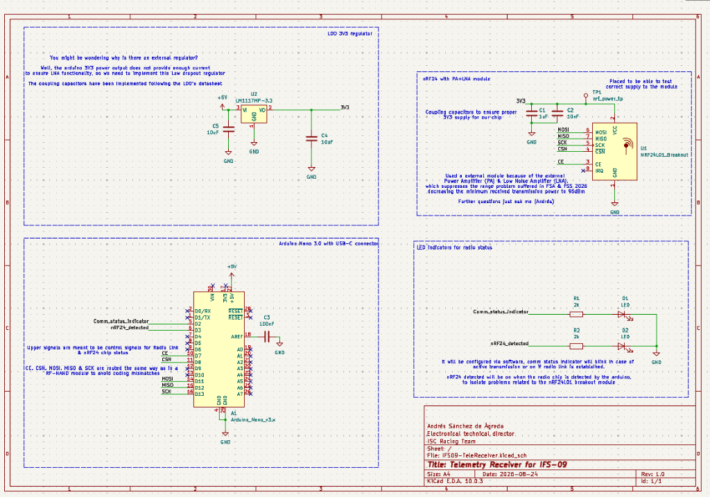
🔍 Click on the schematic preview above to view or download the vector PDF (Schematics-2.0.pdf)
U2) steps down the 5V USB bus rail to an isolated, high-current 3.3V plane (rated up to $800,\text{mA}$).C5) and a $10,\mu\text{F}$ output capacitor (C4) ensuring ripple $< 30,\text{mV}_{p-p}$.U1)C1) and $10,\text{nF}$ (C2) ceramic capacitors placed directly across $V_{CC}$ and $GND$ pins.TP1 (nrf_power_tp) allows direct DMM/oscilloscope measurement of the transceiver power rail.A1)C3) tied from AREF to GND to suppress high-frequency analog reference noise.Comm_status_indicator (D1 LED + $2,\text{k}\Omega$ R1): Connected to Arduino digital pin D2. Controlled via software to blink during active packet reception or remain steady when the RF link is healthy.nRF24_detected (D2 LED + $2,\text{k}\Omega$ R2): Connected to Arduino digital pin D3. Illuminates automatically on setup if radio.isChipConnected() succeeds, providing instantaneous visual feedback isolating socket/transceiver hardware faults from software issues.
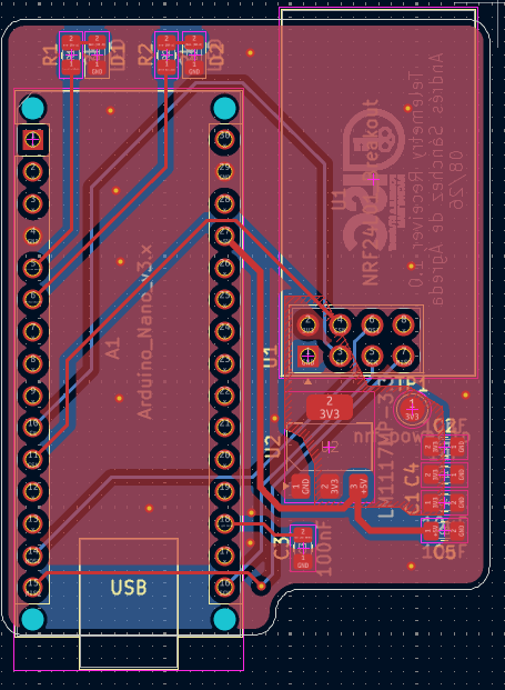
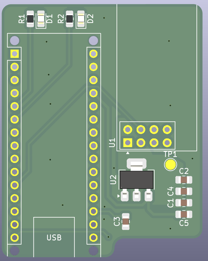
C1–C5) tightly positioned directly below the transceiver header to minimize inductive trace loops.D1, D2) and current-limiting resistors (R1, R2) placed along the top edge for direct visibility.[!IMPORTANT] Authoritative Pinout Notice:
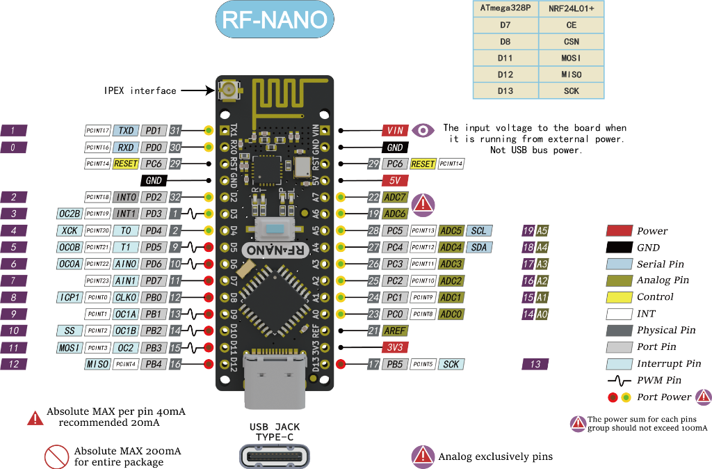
The pinout below is the definitive, verified hardware mapping matchingSchematics-2.0.pdfand the board layout.
CE(Chip Enable):D7(ATmega328PPD7/ Pin 11)CSN(Chip Select Not):D8(ATmega328PPB0/ Pin 12)Comm_status_indicator:D2(PD2/ Pin 5)nRF24_detected:D3(PD3/ Pin 6)- SPI Bus:
MOSI$\rightarrow$D11,MISO$\rightarrow$D12,SCK$\rightarrow$D13
| Subsystem / Function | Signal Name | Arduino Nano Physical Pin | Connected Component & Pin | Functional Description & Notes |
|---|---|---|---|---|
| Power Input (5V Bus) | +5V | Pin 27 (+5V) | LM1117MP-3.3 (Pin 3 VI) | 5V rail from USB-C powers the external LDO regulator (filtered by C5 $10,\mu\text{F}$) |
| Power Output (3.3V Rail) | 3V3 | NC on Arduino (Pin 17) | LM1117 (Pin 2 VO) $\rightarrow$ nRF24 (Pin 2 VCC) | Regulated 3.3V rail from LM1117 powers nRF24L01+ (filtered by C4 $10,\mu\text{F}$, C1 $1,\mu\text{F}$, C2 $10,\text{nF}$, with TP1) |
| Ground Reference | GND | Pins 4 & 29 (GND) | LM1117 (Pin 1), nRF24 (Pin 1), LEDs | Common ground plane for power and high-speed RF return paths |
| Radio Link Status LED | Comm_status_indicator | Pin 5 (D2 / PD2) | LED D1 (Anode) + $2,\text{k}\Omega$ R1 | Software-driven: Blinks on active reception; steady when RF link is established |
| Transceiver Detected LED | nRF24_detected | Pin 6 (D3 / PD3) | LED D2 (Anode) + $2,\text{k}\Omega$ R2 | Hardware validation: ON when radio.isChipConnected() == true on boot |
| Transceiver Chip Enable | CE | Pin 10 (D7 / PD7) | nRF24L01+ (Pin 3 CE) | RX/TX state enable (RF-NANO standard mapping) |
| SPI Chip Select Not | CSN | Pin 11 (D8 / PB0) | nRF24L01+ (Pin 4 CSN) | Active-low SPI select (RF-NANO standard mapping) |
| SPI Master Out Slave In | MOSI | Pin 14 (D11 / PB3) | nRF24L01+ (Pin 6 MOSI) | Hardware SPI Data Line (Arduino $\rightarrow$ nRF24) |
| SPI Master In Slave Out | MISO | Pin 15 (D12 / PB4) | nRF24L01+ (Pin 7 MISO) | Hardware SPI Data Line (nRF24 $\rightarrow$ Arduino) |
| SPI Serial Clock | SCK | Pin 16 (D13 / PB5) | nRF24L01+ (Pin 5 SCK) | Hardware SPI Clock Line |
| Analog Reference Filter | AREF | Pin 18 (AREF) | Capacitor C3 ($100,\text{nF}$) to GND | High-frequency noise suppression for ADC/MCU core |
| Transceiver Interrupt | IRQ | NC on Arduino | nRF24L01+ (Pin 8 IRQ - NC) | Not connected (Polled RX operation used in firmware) |
| USB-Serial Telemetry | TXD / RXD | Pins 1 & 2 (D1/D0) | Integrated USB-C Bridge | High-speed telemetry streaming to PC @ 115200 Baud |
SW/RTT_nano_26/)The official receiver firmware sketch is located in SW/RTT_nano_26/RTT_nano_26.ino.
| Signal / Function | Legacy Prototype (RTT_nano.ino) | New Board (RTT_nano_26.ino) | Notes |
|---|---|---|---|
CE (Chip Enable) | D10 | D7 | Moved to D7 (ATmega328P PD7) |
CSN (Chip Select Not) | D9 | D8 | Moved to D8 (ATmega328P PB0) |
Comm Status LED (D1) | None | D2 | Pulses 40ms on packet reception |
nRF24 Detected LED (D2) | None | D3 | ON when radio.isChipConnected() == true |
PA & LNA Gain | RF24_PA_LOW | RF24_PA_MAX, true | LNA high gain enabled for max sensitivity ($-95,\text{dBm}$) |
#include <SPI.h>
#include <RF24.h>
#include "printf.h"

// Hardware Pin Configuration (IFS09-TeleReceiver)
static const uint8_t PIN_CE           = 7;  // D7 -> nRF24 CE
static const uint8_t PIN_CSN          = 8;  // D8 -> nRF24 CSN
static const uint8_t PIN_LED_COMM     = 2;  // D2 -> Comm Status LED
static const uint8_t PIN_LED_DETECTED = 3;  // D3 -> nRF24 Detected LED

RF24 radio(PIN_CE, PIN_CSN);

void setup() {
    pinMode(PIN_LED_COMM, OUTPUT);
    pinMode(PIN_LED_DETECTED, OUTPUT);
    Serial.begin(115200);

    if (radio.begin() && radio.isChipConnected()) {
        digitalWrite(PIN_LED_DETECTED, HIGH); // Visual confirmation of SPI detection

        radio.setAddressWidth(5);
        radio.setChannel(76);
        radio.setAutoAck(false);
radio.setDataRate(RF24_1MBPS);The project development is documented across three primary engineering artifacts:
| Document | File Link | Description | Status |
|---|---|---|---|
| Design Report | 📄 DR_TE-IFS09-TeleReceiver.pdf | Technical Design Report detailing circuit justifications, component selections, mechanical constraints, and post-fabrication test protocol. | Rev 1.0 (Completed) |
| Work Order | 📄 WO_TE-IFS09-TeleReceiver.pdf | Initial engineering Work Order specifying design requirements, pin mappings, and acceptance criteria. | Rev 1.0 (Released) |
| Schematics Sheet | 📄 Schematics-2.0.pdf | Complete KiCad schematic export with subsystem annotations and decoupling networks. | v2.0 (Final) |
IFS09-TE-TeleReceiver/
├── docs/                              # Documentation Assets
│   └── images/
│       ├── schematic_v2.png           # Exported Schematic v2.0 Image
│       ├── pcb_layout_2d.png          # 2D PCB Layout Routing View
│       ├── pcb_render_3d.png          # 3D PCB Render Model
│       └── rf_nano_pinout.png         # Definitive Pinout Reference
├── IFS09-TeleReceiver/                # KiCad Project Files (KiCad E.D.A. 10.x / 8.x)
│   ├── IFS09-TeleReceiver.kicad_pro   # Project Configuration
│   ├── IFS09-TeleReceiver.kicad_sch   # Schematic Sheet
│   └── IFS09-TeleReceiver.kicad_pcb   # PCB Layout & Netlist
├── SW/                                # Firmware Sketches & Libraries
│   └── RTT_nano_26/                   # Production Telemetry Receiver Firmware
│       ├── RTT_nano_26.ino            # Main Arduino Receiver Sketch
│       └── printf.h                   # Serial Printf Header
├── DR_TE-IFS09-TeleReceiver.pdf       # Official Design Report (Rev 1)
├── WO_TE-IFS09-TeleReceiver.pdf       # Work Order Specification (Rev 1)
├── Schematics-2.0.pdf                 # Latest Exported Schematic Sheet (v2.0)
├── Schematics-1.0.pdf                 # Initial Schematic Sheet (v1.0)
├── .gitignore                         # KiCad and OS ignore rules
└── README.md # Comprehensive DocumentationUpon arrival of manufactured PCB units, the following sequential validation protocol will be executed prior to track deployment:
flowchart LR
    A[1. Power Rail Check (TP1)] --> B[2. SPI & Detection (LED D2)]
    B --> C[3. PuTTY Stream (115200)]
C --> D[4. Dynamic Range Test (≥300m)]TP_5V $\rightarrow$ GND and TP1 (3V3) $\rightarrow$ GND ($> 10,\text{k}\Omega$).TP1 with peak ripple $< 30,\text{mV}_{p-p}$.radio.isChipConnected() == true and illumination of nRF24_detected LED (D3).SCK, MOSI, MISO, CSN, and CE testpoints with logic analyzer/oscilloscope.ISC Racing Team — IFS09 Telemetry Subsystem
| Qty | Value | Footprint | References |
|---|---|---|---|
| 2 | 10uF | Capacitor_SMD:C_0805_2012Metric_Pad1.18x1.45mm_HandSolder | C4, C5 |
| 2 | 2k | Resistor_SMD:R_0805_2012Metric_Pad1.20x1.40mm_HandSolder | R1, R2 |
| 2 | LED | LED_SMD:LED_0805_2012Metric_Pad1.15x1.40mm_HandSolder | D1, D2 |
| 1 | 100nF | Capacitor_SMD:C_0805_2012Metric_Pad1.18x1.45mm_HandSolder | C3 |
| 1 | 10nF | Capacitor_SMD:C_0805_2012Metric_Pad1.18x1.45mm_HandSolder | C2 |
| 1 | 1uF | Capacitor_SMD:C_0805_2012Metric_Pad1.18x1.45mm_HandSolder | C1 |
| 1 | Arduino_Nano_v3.x | Module:Arduino_Nano_WithMountingHoles | A1 |
| 1 | LM1117MP-3.3 | Package_TO_SOT_SMD:SOT-223-3_TabPin2 | U2 |
| 1 | LOGO | ISC_mecanica:CompleteLogo_01 | G*** |
| 1 | NRF24L01_Breakout | RF_Module:nRF24L01_Breakout | U1 |
| 1 | nrf_power_tp | TestPoint:TestPoint_Pad_D2.0mm | TP1 |
QuantumVillage/UncutGem
A prototype Full Stack fully Open Source NV Center Diamond Magnetometer

NYDEREK/LineFollower_GRUZIK2.0-light
GRUZIK2.0 is simple light construction made for "line follower light" competition

BG6LH/FT-81x-BT-DIGI-Adaptor
A PCB Design of Bluetooth DIGI Adaptor for Yaesu FT-817/818 Series Transceivers

shufps/vfd-night-projector-clock
The VFD Night Projector Clock is the first and only (at the moment and to my knowledge 😁) night projecting clock that uses a VFD display.


95lux/aware01
Aarebot is a dynamic realtime sampler built as a Eurorack module. At its core is a stereo tape-style engine with a hot-swapping record/playback buffer - this enables to record and play simultaneously.

porast1/suspension-telemetry
Suspension telemetry system for mountain bike or dirt bike

It measures 38.8 × 48.9 mm and has 2 copper layers, 1.6 mm thick.
14 parts, built around the LM1117MP-3.3. The full list of its parts is on this page, with links to each part's symbol and footprint where PCBKit's library has them.
From the isc-fs/IFS09-TE-TeleReceiver repository on GitHub, at the commit this page was made from: the board is IFS09-TeleReceiver/IFS09-TeleReceiver.kicad_pcb and its schematic IFS09-TeleReceiver/IFS09-TeleReceiver.kicad_sch. PCBKit opens the board in the browser, with nothing to install.
Its repository states no licence, so its author keeps all rights: ask isc-fs before reusing the design.