
2 layers100 × 100 mm
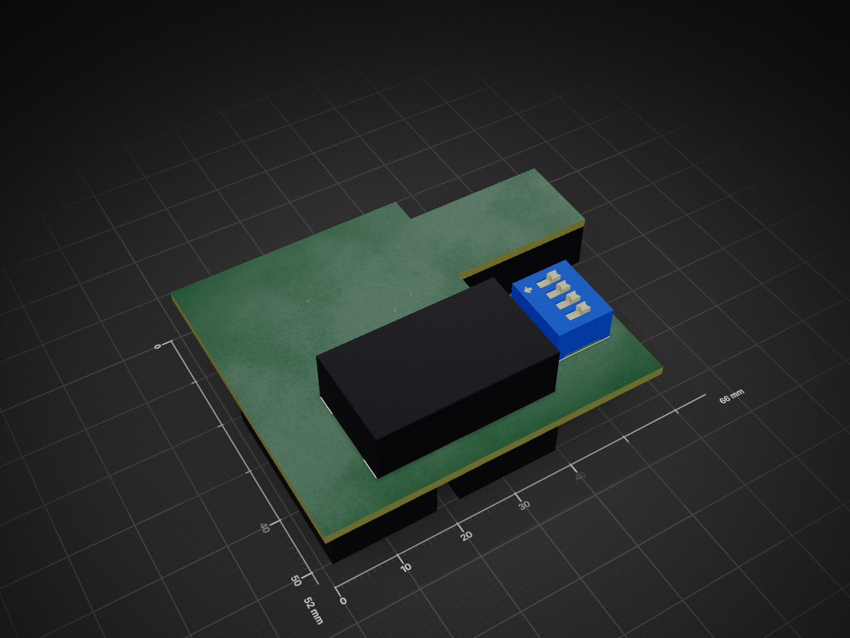
Prueba is an open-source printed circuit board by IoTCloudStudio, from the IoTCloudStudio/HW_Develop repository on GitHub. It is a 2-layer board of 66 × 52 mm with 6 parts on 14 nets, routed with 124 tracks and 5 vias.
Its parts include 5 connectors and 1 switch.
| Qty | Value | Footprint | References |
|---|---|---|---|
| 1 | SIM1 | IoT-JOIN:GCT_SIM5060-6-0-26-00-X_REVC1 | J1 |
| 1 | SIM2 | IoT-JOIN:GCT_SIM5060-6-0-26-00-X_REVC1 | J2 |
| 1 | SIM3 | IoT-JOIN:GCT_SIM5060-6-0-26-00-X_REVC1 | J3 |
| 1 | SIM4 | IoT-JOIN:GCT_SIM5060-6-0-26-00-X_REVC1 | J5 |
| 1 | SIM_Card | IoT-JOIN:SIM_CARD | J4 |
| 1 | SW_DIP | Button_Switch_THT:SW_DIP_SPSTx04_Slide_9.78x12.34mm_W7.62mm_P2.54mm | SW1 |
It measures 66 × 52 mm and has 2 copper layers, 1.6 mm thick.
6 parts. The full list of its parts is on this page, with links to each part's symbol and footprint where PCBKit's library has them.
From the IoTCloudStudio/HW_Develop repository on GitHub, at the commit this page was made from: the board is Productivo/Comunicador Connect/PCB/prueba.kicad_pcb and its schematic Productivo/Cloud UPS/V2/UPSV2concepttocheck.kicad_sch. PCBKit opens the board in the browser, with nothing to install.
Its repository states no licence, so its author keeps all rights: ask IoTCloudStudio before reusing the design.


byrantech/laptop
anyon_e, a highly integrated, high end, open source laptop. Attempt the impossible.


Jcparkyn/dpoint
Open-source digital stylus using camera tracking and inertial measurements

VoronDesign/Voron-Hardware
Cool Hardware designed by the Voron Design group

hoglet67/RGBtoHDMI
Bare-metal Raspberry Pi project that provides pixel-perfect sampling of Retro Computer RGB/YUV video and conversion to HDMI

hackclub/OnBoard
💡 Join 1,000 teenagers and make your first PCB with a $100 grant!

Luos-io/luos_engine
Open-source and real-time orchestrator for cyber-physical-systems, to easily design, test and deploy embedded applications and digital twins.
