2 layers60 × 30 mm

 IM-TechieScientist/librelab1
A low-cost, open source lab instrument that rivals $500 devices
Librelab is an open-source printed circuit board by IM-TechieScientist, from the IM-TechieScientist/librelab repository on GitHub. It is a 2-layer board of 55.5 × 81 mm with 21 parts on 51 nets, routed with 217 tracks and 20 vias.
It is built around the ESP32-C3-WROOM-02-H4 and AMS1117-3.3. Its parts include 7 connectors, 5 capacitors, 3 resistors and 3 ICs. It belongs with the ESP32, RP2040 and RISC-V boards of this library.


LibreLab is a low-cost, open lab instrument for embedded developers: part logic analyser, part mixed-signal scope, part signal generator, part protocol workbench. The goal is simple: make the kind of debug workflow people buy premium USB instruments for available as open hardware and open software at student/hacker-lab pricing.
Current hardware is targeting a PCB+BOM cost below ₹2500, roughly $26.4 at recent INR/USD rates. The next hardware revision is targeting a sub-$50 build with RP2350B, an AD9629-class high-speed ADC path, HSTX-based high-speed data movement toward a USB 3-class host link, and generous PSRAM buffering.
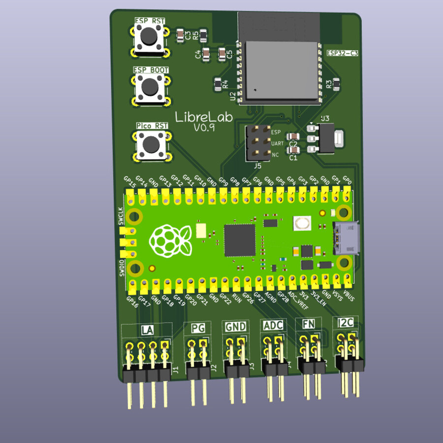 | 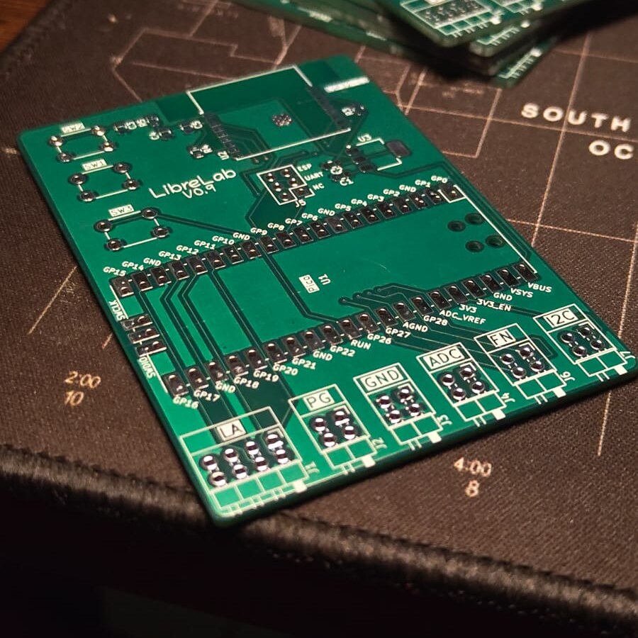 | 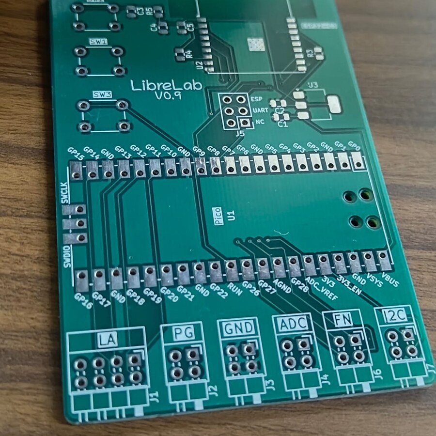 |
| v0.9 board render | fabricated PCB stack | PCB top side |
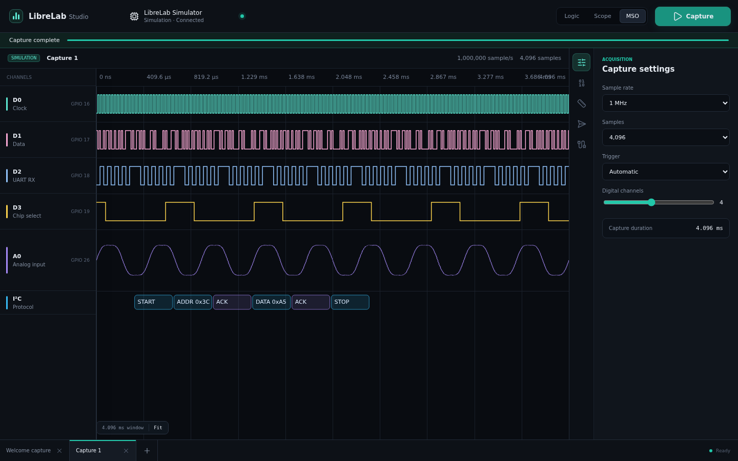
Saleae's current Logic 8 is an 8-channel USB analyser rated at up to 100 MS/s digital capture, 10 MS/s analog capture, 10-bit analog resolution, long PC-streamed captures, 25+ protocol decoders, trigger/search, measurements, automation, and cross-platform software.
LibreLab is aiming at that workflow from the other side of the cost curve:
150 MSPS logic capture on the current RP2350 design path.200 MSPS logic capture under active development.400 MSPS burst-mode capture under active development.$50.The bet is that a carefully designed RP2350-class instrument can be brutally useful for firmware bring-up, protocol debugging, education, and small-lab automation without needing a $500-class box on every desk.
The firmware lives in firmware and currently targets Pico 2/RP2350A. Firmware was originally developed by me as part of GSoC 2026.
Implemented so far:
Useful docs:
The desktop application lives in software and is built with Electron, React, and TypeScript.
Implemented so far:
More:
Run it:
cd software
npm install
npm run dev
Run the browser-rendered GUI for quick UI work:
cd software
npm run dev:renderer -- --host 127.0.0.1The KiCad project lives in pcb/librelab. The current schematic/PCB includes:
pcb/librelab/output/.Near-term:
Hardware vNext:
$50 target cost.| Qty | Value | Footprint | References |
|---|---|---|---|
| 3 | 10k | Resistor_SMD:R_0805_2012Metric | R3, R4, R5 |
| 3 | 10uF | Capacitor_SMD:C_0805_2012Metric | C1, C2, C5 |
| 3 | SW_Push | Button_Switch_THT:SW_PUSH_6mm_H5mm | ESP BOOT, ESP RST, Pico RST |
| 1 | 100n | Capacitor_SMD:C_0805_2012Metric | C4 |
| 1 | 1uF | Capacitor_SMD:C_0805_2012Metric | C3 |
| 1 | ADC headers | Connector_PinHeader_2.54mm:PinHeader_2x02_P2.54mm_Horizontal | J4 |
| 1 | AMS1117-3.3 | Package_TO_SOT_SMD:SOT-223-3_TabPin2 | U3 |
| 1 | Conn_02x03_Counter_Clockwise | Connector_PinHeader_2.54mm:PinHeader_2x03_P2.54mm_Vertical | J5 |
| 1 | ESP32-C3-WROOM-02 | RF_Module:ESP32-C3-WROOM-02 | U2 |
| 1 | FN headers | Connector_PinHeader_2.54mm:PinHeader_2x02_P2.54mm_Horizontal | J6 |
| 1 | GND headers | Connector_PinHeader_2.54mm:PinHeader_2x02_P2.54mm_Horizontal | J3 |
| 1 | I2C headers | Connector_PinHeader_2.54mm:PinHeader_2x02_P2.54mm_Horizontal | J7 |
| 1 | LA headers | Connector_PinHeader_2.54mm:PinHeader_2x04_P2.54mm_Horizontal | J1 |
| 1 | PG headers | Connector_PinHeader_2.54mm:PinHeader_2x02_P2.54mm_Horizontal | J2 |
| 1 | Pico | MCU_RaspberryPi_and_Boards:RPi_Pico_SMD_TH | U1 |
It measures 55.5 × 81 mm and has 2 copper layers, 1.6 mm thick.
21 parts, built around the ESP32-C3-WROOM-02-H4 and AMS1117-3.3. The full list of its parts is on this page, with links to each part's symbol and footprint where PCBKit's library has them.
From the IM-TechieScientist/librelab repository on GitHub, at the commit this page was made from: the board is pcb/librelab/librelab.kicad_pcb and its schematic pcb/librelab/librelab.kicad_sch. PCBKit opens the board in the browser, with nothing to install.
Its repository states no licence, so its author keeps all rights: ask IM-TechieScientist before reusing the design.

nepyope/Project-Homunculus
Project Homunculus is open-source, low-cost hardware for capturing human hand and arm motions. It has two parts.


74th/esp32c3-iot-server-board
Board for converting Grove device to IoT Server using ESP32-C3-WROOM-02.

Domiko7/NexaSeis
Acquisition and processing server for the NexaSeis collaborative seismic network

oltdaniel/PCB_deskDisplay
a small esp32-c3 PCB for an I²C display, NeoPixel and Button for smart home stuff.