2 layers70 × 50 mm
Storage failed
IgorCulafic/PCBSmith
Open-source PCB design tools: KiCad workflows, automatic routing, design review and laser fabrication. Working toward plain-language circuit-to-board design.
104 partsAGPL-3.0

 IgorCulafic/PCBSmith
Open-source PCB design tools: KiCad workflows, automatic routing, design review and laser fabrication. Working toward plain-language circuit-to-board design.
Thermometer R005 is an open-source printed circuit board by IgorCulafic, from the IgorCulafic/PCBSmith repository on GitHub, published under the AGPL-3.0 licence. It is a 2-layer board of 60 × 170 mm with 64 parts on 53 nets, routed with 567 tracks and 99 vias.
It is built around the ESP32-C3-WROOM-02-H4, 74HC595 and AP2112K-3.3, with the SHT31-DIS-F among its other parts. Its parts include 17 resistors, 17 diodes, 8 capacitors, 5 ICs and 3 connectors. It belongs with the sensors and measurement boards and the ESP32 and RISC-V boards of this library.


PCBSmith is an open-source tool for designing printed circuit boards. The long-term goal is to describe a circuit in plain language and get a checked schematic, board layout and manufacturing files. Today it combines a schematic editor prototype with KiCad-based workflows for automatic routing, design review and laser-fabricated boards.
It is under active development. The current tools support supervised engineering work: component choices, design decisions and physical testing still need a person.
Board gallery · Concept to board · Get started · Design workflow · Development
These are retained images from actual design projects. Captions distinguish CAD results, work in progress and physical fabrication.
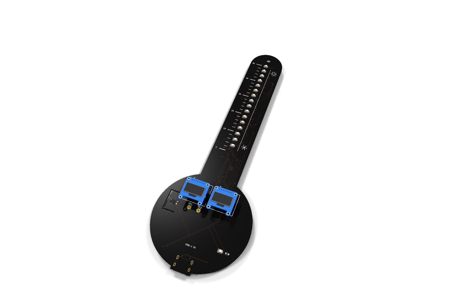 Thermometer 63 components, 53 routed nets and a custom outline. Accepted CAD proof; the render uses some proxy models. |
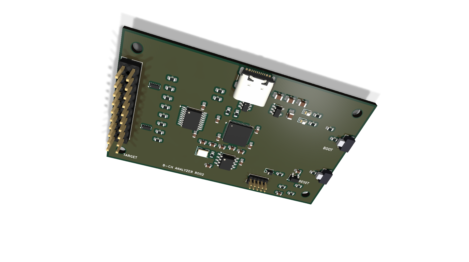 Eight-channel protocol analyzer A more complex controller and input-interface study. Placement prototype; routing and review remain open. |
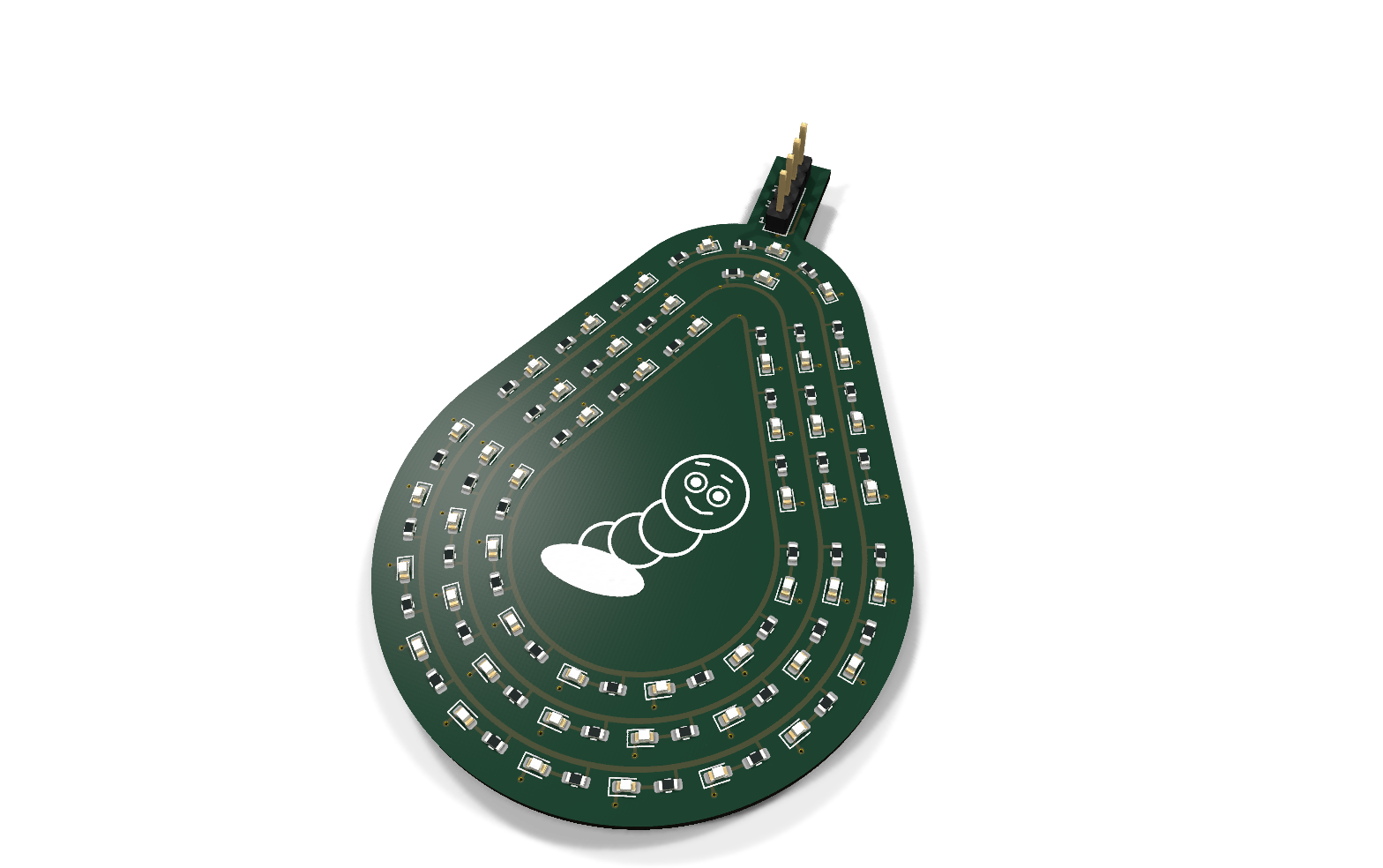 Pear Worm LED rings following a pear outline, with custom silkscreen. Historical design prototype. |
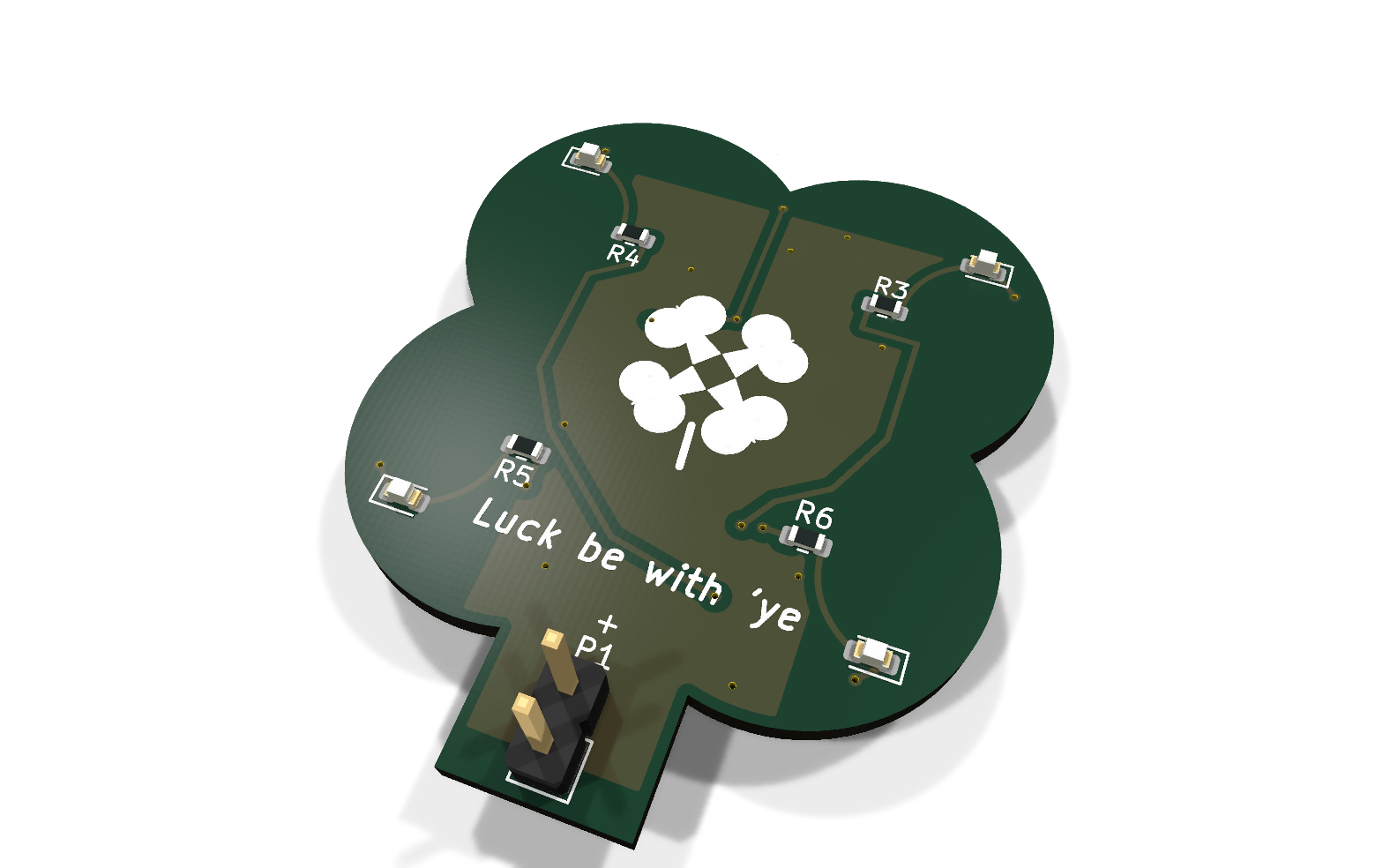 Lucky Clover A compact LED board with a four-lobed outline. Historical design prototype. |
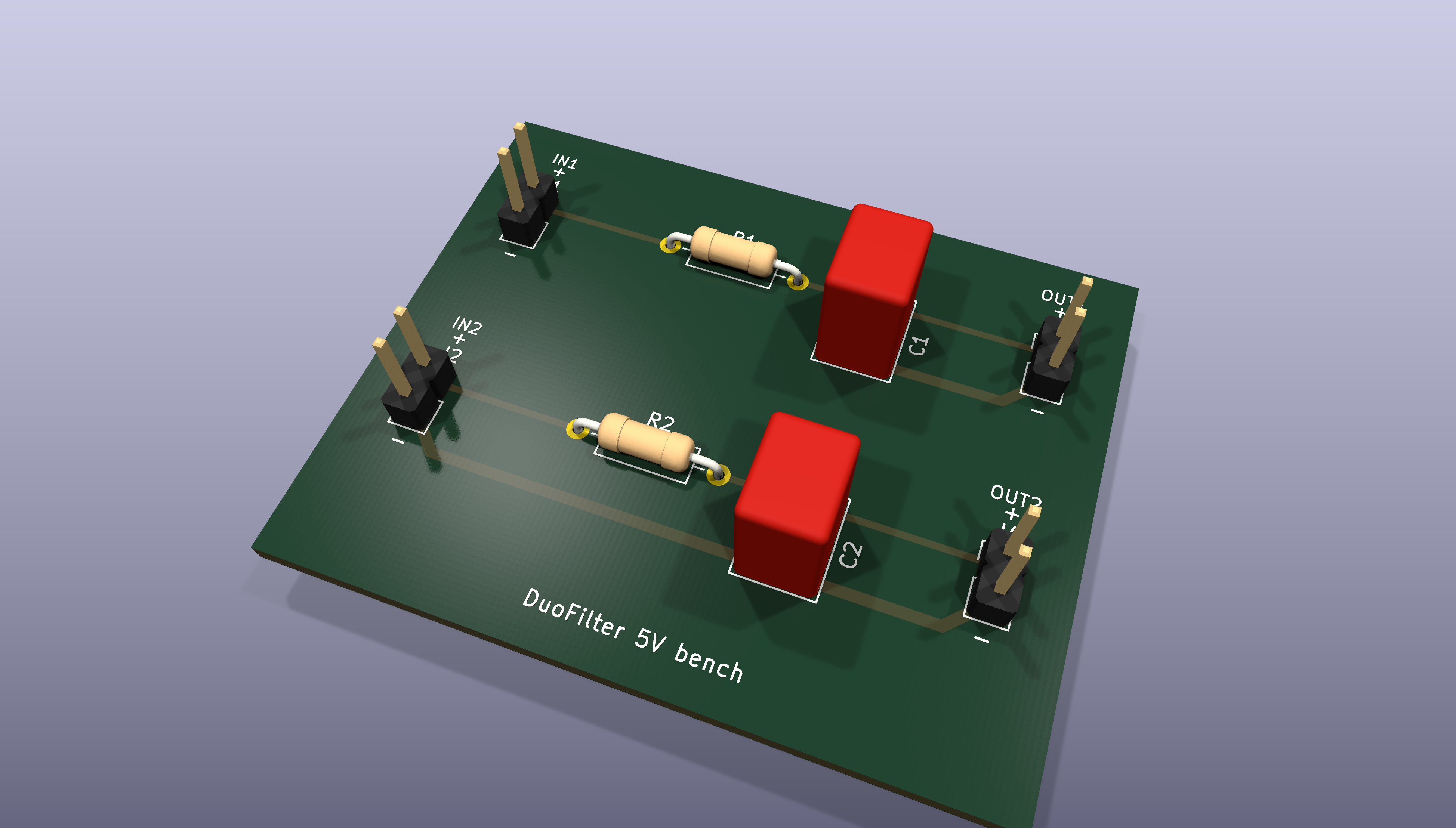 DuoFilter Two-sided RC filter: automatic routing, a resistor revision and a checked CAD handover. |
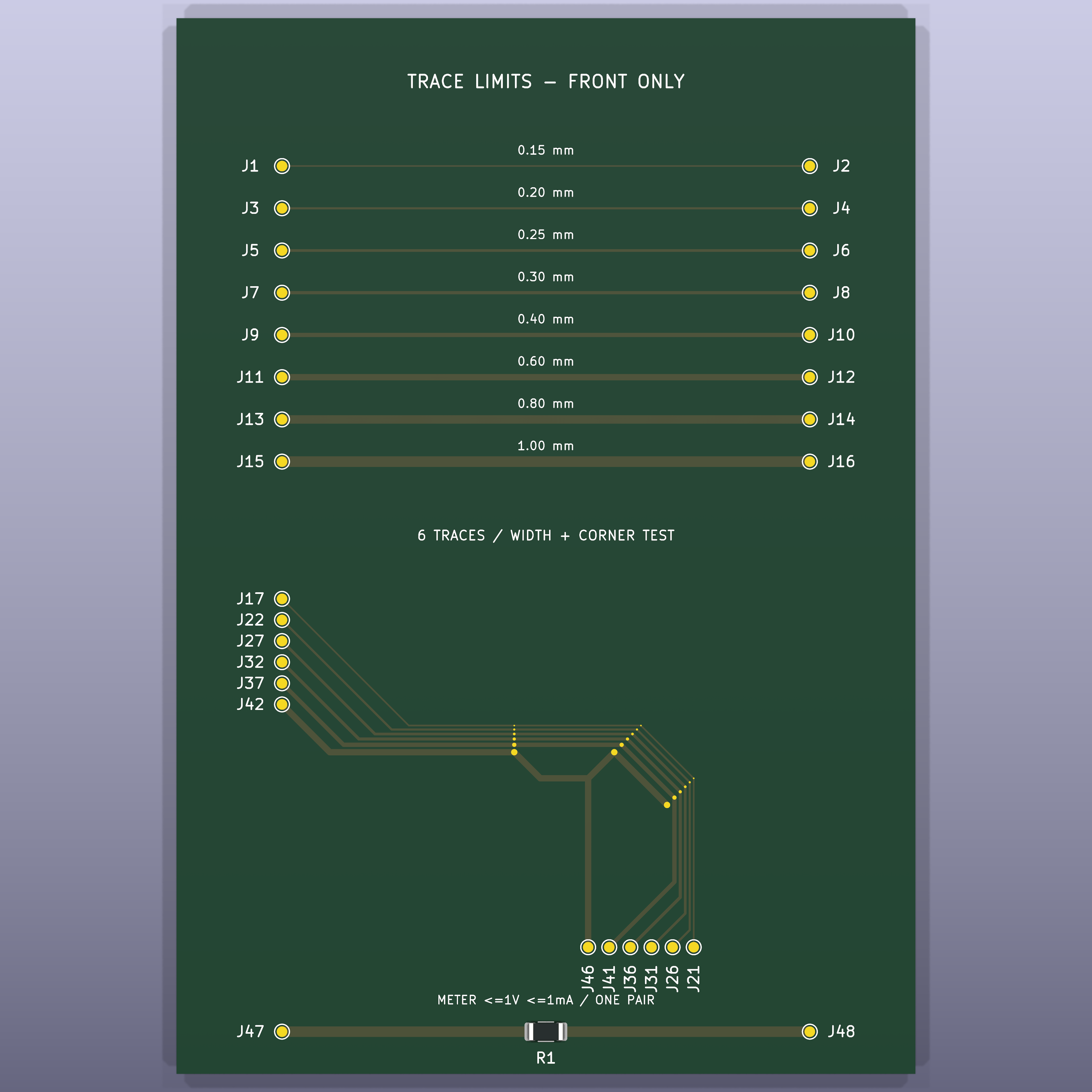 TraceLimits — recent laser test 0.15–1.00 mm traces, a six-net corner test and two isolation widths. CAD handover complete; process measurements pending. |
The full gallery includes routing views, laser-artwork comparisons and a two-sided plated-hole test coupon.
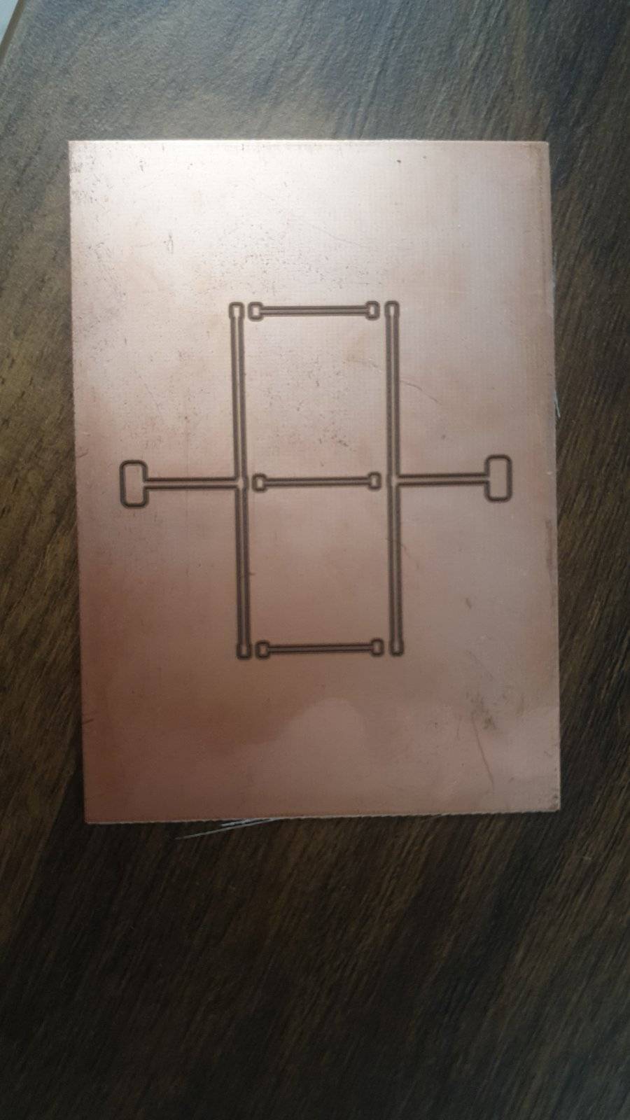
An early single-sided laser test, photographed by the builder. The builder reported that the process worked and requested wider isolation channels for the next tests. This is a physical fabrication result; the newer trace-width and plating coupons are still awaiting measurements.
The main fabrication scope is single- and two-sided boards. Laser CAM currently supports documented straight-track/simple-pad geometry; unsupported cases are reported. See current scope and limits for the details. A clean CAD check does not establish component fit, circuit operation or a qualified fabrication process.
A finished render is one step in the process. Here is the same TraceLimits board moving from a dimensioned concept to real copper geometry and laser artwork:
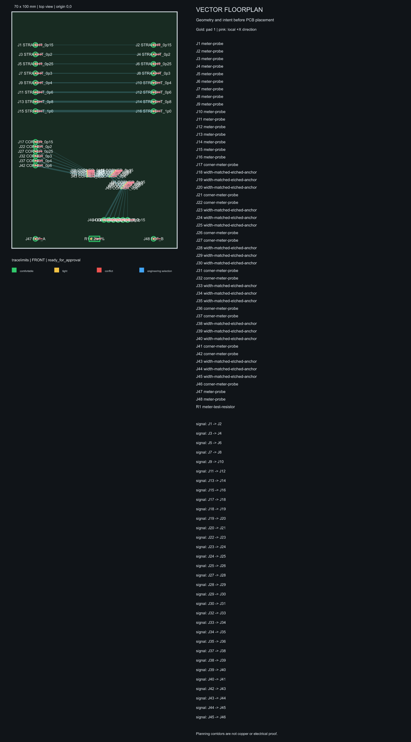 1. Concept and placement intent Board dimensions, probe positions and routing corridors. | 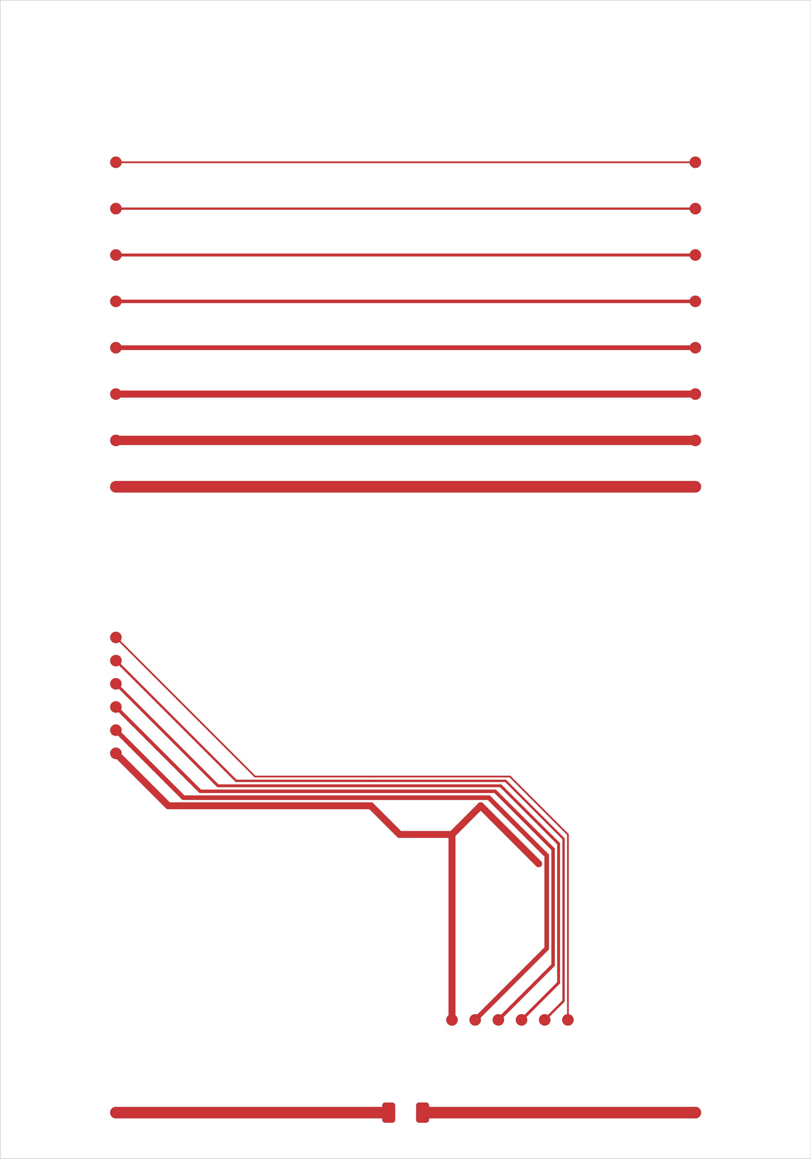 2. Routed and checked PCB 16 nets, 46 segments, front copper only. | 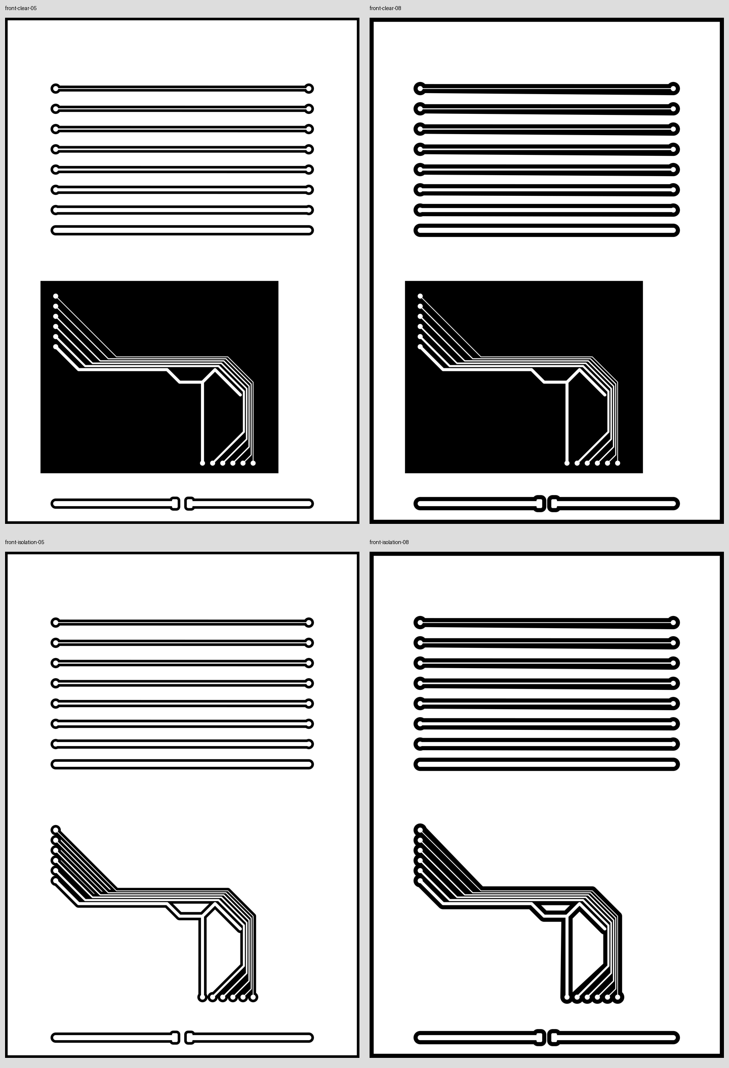 3. Fabrication artwork Compare channel widths and background-copper removal. |
The illustrated development walkthrough also shows the schematic, 3D inspection, pad-only coating mask and interactive BOM, then explains the physical measurements still to come. Download the working BOM example to open locally in a browser.
The maintained development setup is Python 3.12.12, uv 0.11.23 and KiCad 10 with its symbol and footprint libraries. See development setup for native-tool paths, optional dependencies and verification.
git clone https://github.com/IgorCulafic/PCBSmith.git
cd PCBSmith
uv sync --frozen --all-extras --python 3.12.12
uv run --frozen --all-extras pcbsmith-gui
pcbsmith-gui opens the schematic editor prototype. Native board generation, review, routing and delivery use the separate production CLI workflow.
To see CLI commands or run the standard developer checks:
uv run --frozen --all-extras pcbsmith --help
uv run --frozen --all-extras python -B tools/verify.py --output .pcbsmith/verification/first-run
Choose a new verification output directory for each run. The standard checks cover the dependency lock, lint, types, architecture, workflow entry points and ordinary tests. The optional deep profile also requires live KiCad/ngspice tools.
PCBSmith is licensed under AGPL-3.0-or-later. Bundled KiCad library assets retain their own terms; see third-party notices.
| Qty | Value | Footprint | References |
|---|---|---|---|
| 17 | RED-0805 | LED_SMD:LED_0805_2012Metric | D1, D2, D3, D4, D5, D6, D7, D8, D10, D11, D12, D13, D14, D15, D16, D17 +1 |
| 16 | 270R | Resistor_SMD:R_0603_1608Metric | R1, R2, R3, R4, R5, R6, R7, R8, R9, R10, R11, R12, R13, R14, R15, R16 |
| 5 | 100n | Capacitor_SMD:C_0603_1608Metric | C2, C3, C4, C7, CEN1 |
| 4 | 10k | Resistor_SMD:R_0603_1608Metric | REN1, ROE1, RS1, RS2 |
| 4 | 4.7k | Resistor_SMD:R_0603_1608Metric | RI1, RI2, RI3, RI4 |
| 2 | 1uF X7R | Capacitor_SMD:C_0805_2012Metric | C5, C6 |
| 2 | 5.1k | Resistor_SMD:R_0603_1608Metric | RCC1, RCC2 |
| 2 | 74HC595 | Package_SO:TSSOP-16_4.4x5mm_P0.65mm | U2, U3 |
| 1 | 10uF | Capacitor_SMD:C_0805_2012Metric | C1 |
| 1 | 1k | Resistor_SMD:R_0603_1608Metric | R17 |
| 1 | 500mA polyfuse | Fuse:Fuse_1206_3216Metric | F1 |
| 1 | AP2112K-3.3 | Package_TO_SOT_SMD:SOT-23-5 | U5 |
| 1 | ESP32-C3-WROOM-02 | RF_Module:ESP32-C3-WROOM-02 | U1 |
| 1 | M3 | MountingHole:MountingHole_3.2mm_M3 | H1 |
| 1 | OLED 0.49in HUM | Connector_PinHeader_2.54mm:PinHeader_1x04_P2.54mm_Vertical | J3 |
| 1 | OLED 0.49in TEMP | Connector_PinHeader_2.54mm:PinHeader_1x04_P2.54mm_Vertical | J2 |
| 1 | SHT31-DIS | Sensor_Humidity:Sensirion_DFN-8-1EP_2.5x2.5mm_P0.5mm_EP1.1x1.7mm | U4 |
| 1 | TP 3V3 | TestPoint:TestPoint_THTPad_D2.0mm_Drill1.0mm | TP1 |
| 1 | TP GND | TestPoint:TestPoint_THTPad_D2.0mm_Drill1.0mm | TP2 |
| 1 | USB-C 2.0 16P | Connector_USB:USB_C_Receptacle_GCT_USB4105-xx-A_16P_TopMnt_Horizontal | J1 |
It measures 60 × 170 mm and has 2 copper layers, 1.6 mm thick.
64 parts, built around the ESP32-C3-WROOM-02-H4, 74HC595, AP2112K-3.3 and SHT31-DIS-F. The full list of its parts is on this page, with links to each part's symbol and footprint where PCBKit's library has them.
From the IgorCulafic/PCBSmith repository on GitHub, at the commit this page was made from: the board is outputs/thermometer-production-r005/Thermometer_R005.kicad_pcb. PCBKit opens the board in the browser, with nothing to install.
Its repository publishes it under the AGPL-3.0 licence: you may reuse it on that licence's terms (keep the author's notice, and for a copyleft licence share your changes alike).
IgorCulafic/PCBSmith
Open-source PCB design tools: KiCad workflows, automatic routing, design review and laser fabrication. Working toward plain-language circuit-to-board design.

minhtenlado/esp32-4-channel-relays-temp
⚡ Open-source ESP32 4-Channel Opto-Isolated Relay Controller board designed in KiCad.

unicab369/ESP-MESS
I am building a Wireless Bridge System that can manage multiple devices using a variety of wireless technologies.


Eswar-426/ESP32-Industrial-Sensor-Controller
A custom, compact PCB designed in KiCad 10 for an ESP32-based industrial temperature and humidity monitoring system.

Gecesars/01-plataforma-telemetria-broadcast
Plataforma Unificada de Telemetria de Estação Transmissora — baseline técnica e acompanhamento do projeto


kaushalch1/air-monitor
this is a portable air quality monitoring device designed to measure particulate matter and environmental conditions in real time.
