

4 layers35 × 25 mm

 igilarranz/MotionSense-IMU
2-layer USB-C powered LSM6DSM IMU breakout board designed in KiCad
MotionSense IMU is an open-source printed circuit board by igilarranz, from the igilarranz/MotionSense-IMU repository on GitHub. It is a 2-layer board of 35.4 × 27.5 mm with 12 parts on 18 nets, routed with 146 tracks and 9 vias.
It is built around the AP2112K-3.3 and LSM6DSM. Its parts include 4 capacitors, 4 resistors, 2 ICs and 2 connectors. It belongs with the sensors and measurement boards of this library.
MotionSense IMU is a custom 2-layer PCB built around the ST LSM6DSM 6-axis accelerometer and gyroscope.
The board takes 5 V from USB-C, regulates it to 3.3 V, and breaks out the IMU's I2C interface and interrupt signal through a 5-pin header.
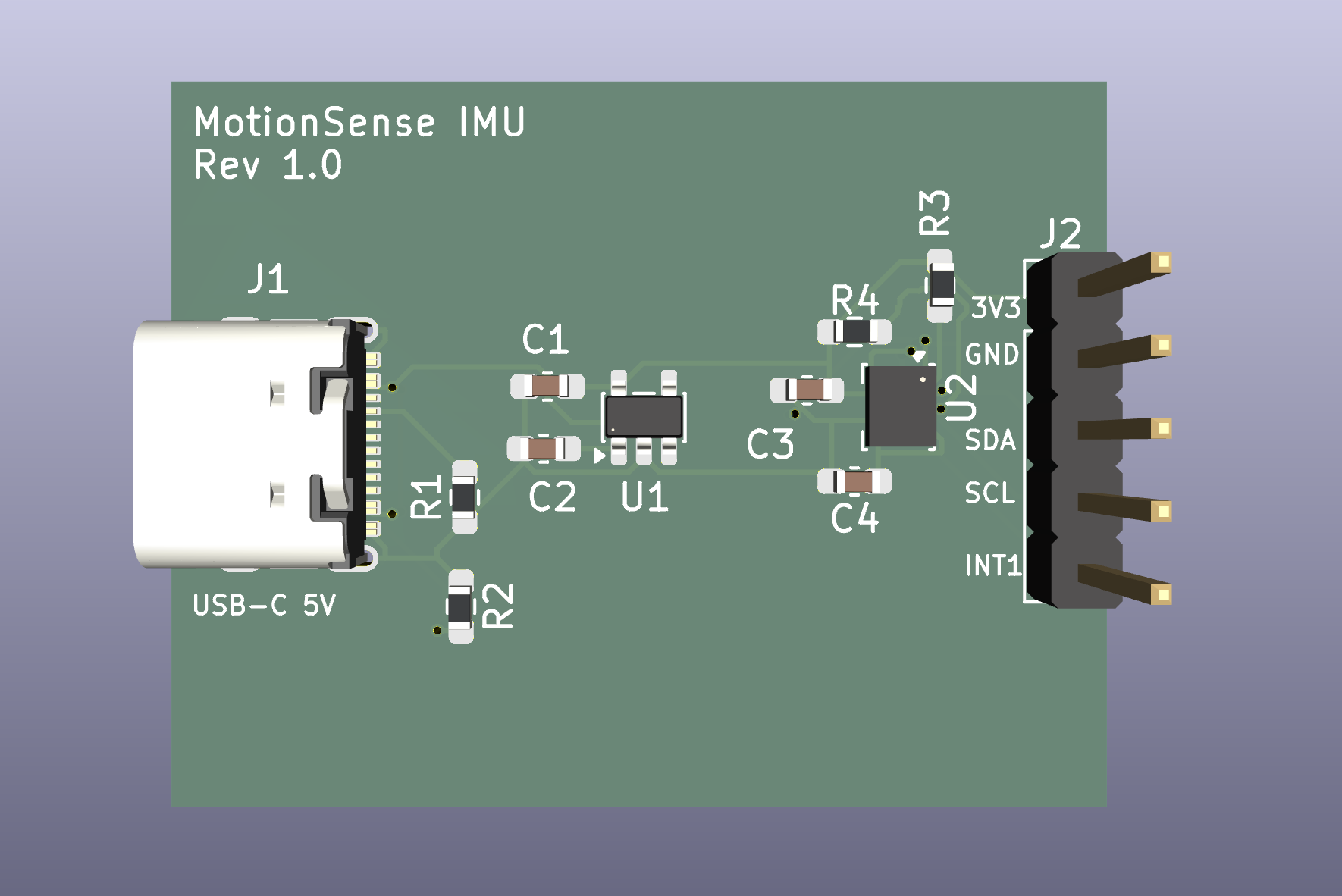
| Pin | Signal |
|---|---|
| 1 | 3V3 |
| 2 | GND |
| 3 | SDA |
| 4 | SCL |
| 5 | INT1 |
The schematic and PCB were designed in KiCad.
During routing, I experimented with Quilter and Freerouting before bringing the design back into KiCad for final cleanup and verification.
The final design passes KiCad DRC with:
Gerber and drill files were generated and inspected before manufacturing.
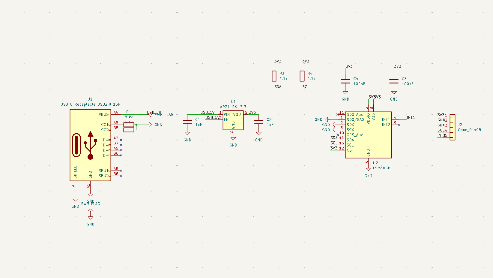
The schematic includes the USB-C power input, AP2112K 3.3 V regulator, LSM6DSM IMU, I2C pull-up resistors, decoupling capacitors, and J2 breakout header.
The editable KiCad schematic is available in MotionSense_IMU.kicad_sch.
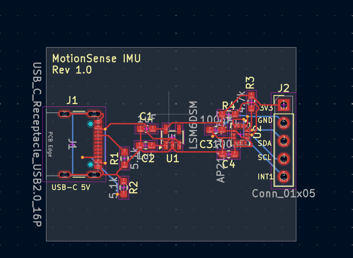
The board is a 2-layer design with USB-C power input on one side and the I2C breakout header on the opposite side.
Rev 1 was submitted to JLCPCB for fabrication and assembly in August 2026.
Five PCBs were ordered, with two boards receiving component assembly.
The 1×5 J2 header is intentionally left unpopulated and will be soldered manually during bring-up.
MotionSense_IMU.kicad_pcb — KiCad PCB layoutMotionSense_IMU.kicad_pro — KiCad projectMotionSense_IMU.kicad_sch — KiCad schematicBOM.csv — bill of materialsMotionSense_IMU_Rev1_Gerbers.zip — Gerber and drill filespcb_3D.png — 3D board renderpcb_layout.png — PCB layout imageschematic.png — schematic imageThe Rev 1 Gerber and drill files used for manufacturing are included in the repository.
Rev 1 has been ordered for fabrication and assembly.
The PCB design and manufacturing files are complete. The next stage is hardware bring-up and firmware validation once the assembled boards arrive.
WHO_AM_I register to confirm communication.The goal of this project is to work through the complete PCB development process, from schematic capture and component selection through layout, manufacturing, assembly, and hardware validation.
| Qty | Value | Footprint | References |
|---|---|---|---|
| 2 | 100nF | Capacitor_SMD:C_0603_1608Metric_Pad1.08x0.95mm_HandSolder | C3, C4 |
| 2 | 1uF | Capacitor_SMD:C_0603_1608Metric_Pad1.08x0.95mm_HandSolder | C1, C2 |
| 2 | 4.7k | Resistor_SMD:R_0603_1608Metric_Pad0.98x0.95mm_HandSolder | R3, R4 |
| 2 | 5.1k | Resistor_SMD:R_0603_1608Metric_Pad0.98x0.95mm_HandSolder | R1, R2 |
| 1 | AP2112K-3.3 | Package_TO_SOT_SMD:SOT-23-5 | U1 |
| 1 | Conn_01x05 | Connector_PinHeader_2.54mm:PinHeader_1x05_P2.54mm_Vertical | J2 |
| 1 | LSM6DSM | Package_LGA:LGA-14_3x2.5mm_P0.5mm_LayoutBorder3x4y | U2 |
| 1 | USB_C_Receptacle_USB2.0_16P | Connector_USB:USB_C_Receptacle_GCT_USB4105-xx-A_16P_TopMnt_Horizontal | J1 |

sawaiz/artDecoEarrings
Shimmering electronic earrings in the Art Deco style.

Xasin/TapBadgeV2
The second, far more ambitious version of the TapBadge wearable


r3dpath/RpiFly_Hardware
While most of the functionality here has been tested to work theres certainally some marginal design decisions, just beware.


benmcnelly/walter-hardware
This repository contains all hardware information about Walter and shields

gavin4d/PPG-Watch
Smart watch with a photoplethysmography analog front end and e-paper display
It measures 35.4 × 27.5 mm and has 2 copper layers, 1.6 mm thick.
12 parts, built around the AP2112K-3.3 and LSM6DSM. The full list of its parts is on this page, with links to each part's symbol and footprint where PCBKit's library has them.
From the igilarranz/MotionSense-IMU repository on GitHub, at the commit this page was made from: the board is MotionSense_IMU.kicad_pcb and its schematic MotionSense_IMU.kicad_sch. PCBKit opens the board in the browser, with nothing to install.
Its repository states no licence, so its author keeps all rights: ask igilarranz before reusing the design.