4 layers105 × 105 mm
Dev real
iamdarshg/dev-board
Self-contained project: board + schematics + libraries. Unzip anywhere and open dev-real.kicadpro in KiCad 9.
318 parts1
 iamdarshg/dev-board1
Self-contained project: board + schematics + libraries. Unzip anywhere and open dev-real.kicadpro in KiCad 9.
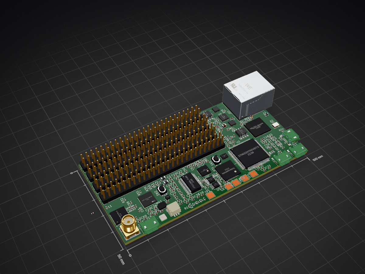
Dev board is an open-source printed circuit board by iamdarshg, from the iamdarshg/dev-board repository on GitHub. It is a 4-layer board of 100 × 50 mm with 177 parts on 322 nets, routed with 256 tracks and 17 vias.
It is built around the LAN8742A-CZ, MP4541GN-Z and AD9609BCPZRL7-80, with the ENS161-BLGT LGA9 T&R 1K5, FT232RNL-TUBE and IWRL6432BDBAAMFR among its other parts. Its parts include 90 capacitors, 47 resistors, 17 ICs, 11 connectors and 3 inductors. It belongs with the microcontroller boards boards and the RP2350 and STM32 boards of this library.


Self-contained project: board + schematics + libraries. Unzip anywhere and open
dev-real.kicad_pro in KiCad 9.
Board is at 0 DRC errors and 0 unconnected items — fully routed.
All 14 unconnected items from the previous pass (was 499 originally) have
been resolved, including the last 6 hold-outs around the U13 radar BGA
corner (GND ball M12, an In2/GND stub near (56.9, 16.0), C34 pad 1, U21 pad
26, a split GND plane island on In1, and an NRESET In1↔F gap) — these needed
hand-routing (via-in-pad style connections plus small shoves of a couple of
neighboring nets — FT_RXD, GPIO_4 — that were routed directly under the
affected pads) since the escape-track congestion in that corner defeats the
interactive shove router's default settings. Inspect → Design Rules Checker → Run DRC now reports 0 errors, 0 unconnected with zones
refilled.
If future edits reintroduce unconnected items, the same workflow applies:
dev-real.kicad_pro → PCB Editor.Route → Interactive Router Settings… → set Mode: Shove (Walk Around
struggles near the U13 BGA corner, where several nets route directly
under neighboring balls).Inspect → Design Rules Checker → Run DRC, open the Unconnected
Items tab, double-click an item to zoom to it.X → route → double-click to finish. Press V
mid-route to drop a via and switch layers.B to refill all zones before the final DRC check — stale zone
fill after a track/via edit can itself show up as a false clearance
violation until refilled./AD9609/SCOPE_BIAS has no DC reference anywhere in the schematic — the net
floats on the real board. Open ad9609bcpzrl7_80_breakout.kicad_sch and define
the intended bias source, then Tools → Update PCB from Schematic (F8).
After any edit: press B to refill zones, then Inspect → Design Rules Checker → Run DRC and confirm it still reads 0 errors, 0 unconnected
before Ctrl+S.
Signal 0.127 mm / vias 0.254 mm with 0.127 mm drill / clearance 0.08 mm / min through-drill 0.127 mm. Power rails run 0.2–0.5 mm. The 0.2/0.1 vias on this board are microvias — place a new through-via that small and DRC will (correctly) reject it.
dev-real.kicad_pcb — the boarddev-real.kicad_pro — project + design rules (keep beside the board;
without it KiCad invents default rules and DRC becomes meaningless)dev-real.kicad_sch + 8 hierarchical sheets — full schematicfp-lib-table, sym-lib-table + the custom symbol/footprint libraries they
reference (AD9609, IWRL6432, MM8108, THS8136, XCC1352, ICM-42670, ENS161,
MMC5633, plus the project's .pretty footprint dirs)Verified standalone: netlist exports all 318 components across the 9-sheet hierarchy, and DRC output is identical to the working copy.
Full history, method, DRC report, renders and the routing scripts stay in
D:\dev-real-updated\dev-real-updated\dev-real-routing-finish\.
| Qty | Value | Footprint | References |
|---|---|---|---|
| 47 | 100n | Capacitor_SMD:C_0402_1005Metric | C11, C12, C13, C14, C15, C16, C17, C18, C20, C21, C22, C23, C24, C26, C27, C33 +31 |
| 17 | 10u | Capacitor_SMD:C_0402_1005Metric | C25, C28, C30, C31, C34, C35, C46, C53, C58, C62, C68, C70, C72, C74, C76, C83 +1 |
| 12 | 10k | Resistor_SMD:R_0402_1005Metric | R11, R12, R13, R17, R18, R19, R22, R23, R26, R27, R28, R29 |
| 8 | 2.2u | Capacitor_SMD:C_0402_1005Metric | C47, C48, C69, C71, C73, C78, C79, C80 |
| 7 | 1k | Resistor_SMD:R_0402_1005Metric | R2, R4, R6, R45, R46, R47, R48 |
| 6 | 75 | Resistor_SMD:R_0402_1005Metric | R32, R33, R34, R42, R43, R44 |
| 5 | 1u | Capacitor_SMD:C_0402_1005Metric | C29, C32, C36, C37, C60 |
| 5 | TestPoint | TestPoint:TestPoint_Pad_3.0x3.0mm | TP1, TP2, TP3, TP4, TP5 |
| 4 | 2.2k | Resistor_SMD:R_0402_1005Metric | R25, R39, R40, R41 |
| 4 | 49.9 | Resistor_SMD:R_0402_1005Metric | R35, R36, R37, R38 |
| 3 | 10n | Capacitor_SMD:C_0402_1005Metric | C39, C40, C81 |
| 3 | 33 | Resistor_SMD:R_0402_1005Metric | R3, R49, R50 |
| 2 | 100k | Resistor_SMD:R_0402_1005Metric | R15, R16 |
| 2 | 15p | Capacitor_SMD:C_0402_1005Metric | C3, C4 |
| 2 | 27 | Resistor_SMD:R_0402_1005Metric | R7, R8 |
| 2 | 4.7k | Resistor_SMD:R_0402_1005Metric | R9, R10 |
| 2 | 4.7u | Capacitor_SMD:C_0402_1005Metric | C9, C10 |
| 2 | 4.7u | RP2350_80QFN_minimal:C_0402_1005Metric_small_pads | C6, C7 |
| 2 | DNP / not used | Connector_USB:USB_Micro-B_Amphenol_10103594-0001LF_Horizontal | J13, J14 |
| 2 | MP4541GN-Z | MP4541GN-Z:SOIC127P600X170-9N | IC5, IC10 |
| 2 | SW_Push | Button_Switch_SMD:SW_Push_1P1T_NO_Vertical_Wuerth_434133025816 | SW1, SW2 |
| 2 | TPS40304ADRCR | TPS40304ADRCR:TPS40304ADRCR | IC7, IC9 |
| 1 | 0R | Resistor_SMD:R_0402_1005Metric | R30 |
| 1 | 0R/DNP | Resistor_SMD:R_0402_1005Metric | R51 |
| 1 | 10u | Capacitor_SMD:C_0805_2012Metric | C19 |
| 1 | 10uH | Inductor_SMD:L_0805_2012Metric | L2 |
| 1 | 12.1k | Resistor_SMD:R_0402_1005Metric | R24 |
| 1 | 1n | Capacitor_SMD:C_0402_1005Metric | C89 |
| 1 | 22p | Capacitor_SMD:C_0402_1005Metric | C91 |
| 1 | 3.3u | RP2350_80QFN_minimal:L_pol_2016 | L1 |
| 1 | 3.8k | Resistor_SMD:R_0402_1005Metric | R31 |
| 1 | 330k | Resistor_SMD:R_0402_1005Metric | R14 |
| 1 | 4.7uH | Inductor_SMD:L_0805_2012Metric | L3 |
| 1 | 47n | Capacitor_SMD:C_0402_1005Metric | C95 |
| 1 | ABM8-272-T3 | Crystal:Crystal_SMD_3225-4Pin_3.2x2.5mm | Y1 |
| 1 | AD9609BCPZRL7-80 | AD9609BCPZRL7-80:QFN50P500X500X100-33N | IC1 |
| 1 | Conn_02x26_Odd_Even | Connector_PinHeader_2.54mm:PinHeader_2x26_P2.54mm_Vertical | J2 |
| 1 | ENS161-BLGT_LGA9_T&R_1k5 | ENS161-BLGT_LGA9_T&R_1k5:ENS161BLGTLGA9TR1k5 | IC2 |
| 1 | FT232RNL-TUBE | Package_SO:SSOP-28_5.3x10.2mm_P0.65mm | U7 |
| 1 | HS/IWRL Fabric Breakout | Connector_PinHeader_2.54mm:PinHeader_2x26_P2.54mm_Vertical | J9 |
| 1 | ICM-42670-P | ICM-42670-P:ICM42670P | IC3 |
| 1 | IM69D120 | Sensor_Audio:Infineon_PG-LLGA-5-1 | MK1 |
| 1 | IWRL USB PROGRAM | Connector_USB:USB_Micro-B_Amphenol_10103594-0001LF_Horizontal | J15 |
| 1 | IWRL6432BDBAAMFR | IWRL6432BDBAAMFR:BGA102C50P12X12_645X645X97 | IC4 |
| 1 | LAN8742A | Package_DFN_QFN:VQFN-24-1EP_4x4mm_P0.5mm_EP2.5x2.5mm_ThermalVias | U4 |
| 1 | LPS22HH | Package_LGA:ST_HLGA-10_2x2mm_P0.5mm_LayoutBorder3x2y | U2 |
| 1 | MCP6D11T-E/MS | MCP6D11T:MCP6D11T-E_MSOP-8_3x3mm_P0.65mm | U6 |
| 1 | PGA113 | Package_SO:TSSOP-10_3x3mm_P0.5mm | U5 |
| 1 | RJ45 / 8P8C LED | Connector_RJ:RJ45_Wuerth_7499010211A_Horizontal | J10 |
| 1 | RP2350 USB PROGRAM | Connector_USB:USB_Micro-B_Amphenol_10103594-0001LF_Horizontal | J12 |
| 1 | RP2350_80QFN | RP2350_80QFN_minimal:RP2350-QFN-80-1EP_10x10_P0.4mm_EP3.4x3.4mm_ThermalVias | U1 |
| 1 | SM03B-SRSS-TB | Connector_JST:JST_SH_SM03B-SRSS-TB_1x03-1MP_P1.00mm_Horizontal | J4 |
| 1 | SMA_RF_LAUNCH | Connector_Coaxial:SMA_Amphenol_132134-10_Vertical | J11 |
| 1 | STM32H7 GPIO/Fabric Breakout A | Connector_PinHeader_2.54mm:PinHeader_2x26_P2.54mm_Vertical | J5 |
| 1 | STM32H7 GPIO/Fabric Breakout B | Connector_PinHeader_2.54mm:PinHeader_2x26_P2.54mm_Vertical | J6 |
| 1 | STM32H750VBTx | Package_QFP:LQFP-100_14x14mm_P0.5mm | U3 |
| 1 | THS8136IPHPR | THS8136IPHPR:QFP50P900X900X120-49N | IC6 |
| 1 | XCC1352R1F3RGZR | XCC1352R1F3RGZR:QFN50P700X700X100-49N-D | IC8 |
It measures 100 × 50 mm and has 4 copper layers, 1.6 mm thick.
177 parts, built around the LAN8742A-CZ, MP4541GN-Z, AD9609BCPZRL7-80 and ENS161-BLGT LGA9 T&R 1K5. The full list of its parts is on this page, with links to each part's symbol and footprint where PCBKit's library has them.
From the iamdarshg/dev-board repository on GitHub, at the commit this page was made from: the board is dev_board.kicad_pcb and its schematic IWRL6432BDBAAMFR_breakout.kicad_sch. PCBKit opens the board in the browser, with nothing to install.
Its repository states no licence, so its author keeps all rights: ask iamdarshg before reusing the design.
iamdarshg/dev-board
Self-contained project: board + schematics + libraries. Unzip anywhere and open dev-real.kicadpro in KiCad 9.

eagletrt/bms-monitor
Slave BMS module to monitor 24s cells voltages and temperatures.


ViratS-best/Aesthetiocizer
Xiao car AI project: firmware inference, embedded model assets, and hardware design.

Jochen0x90h/LedControl
Controller for LED strips based on WS2812 with display based on SSD1306
