2 layers41.3 × 24.9 mm
Pcb v2
hvtran21/SWAN
UMass Amherst ECE Senior Design Project - SWAN - A more secure and user centered solution to wireless access control.
12 parts
 hvtran21/SWAN
UMass Amherst ECE Senior Design Project - SWAN - A more secure and user centered solution to wireless access control.
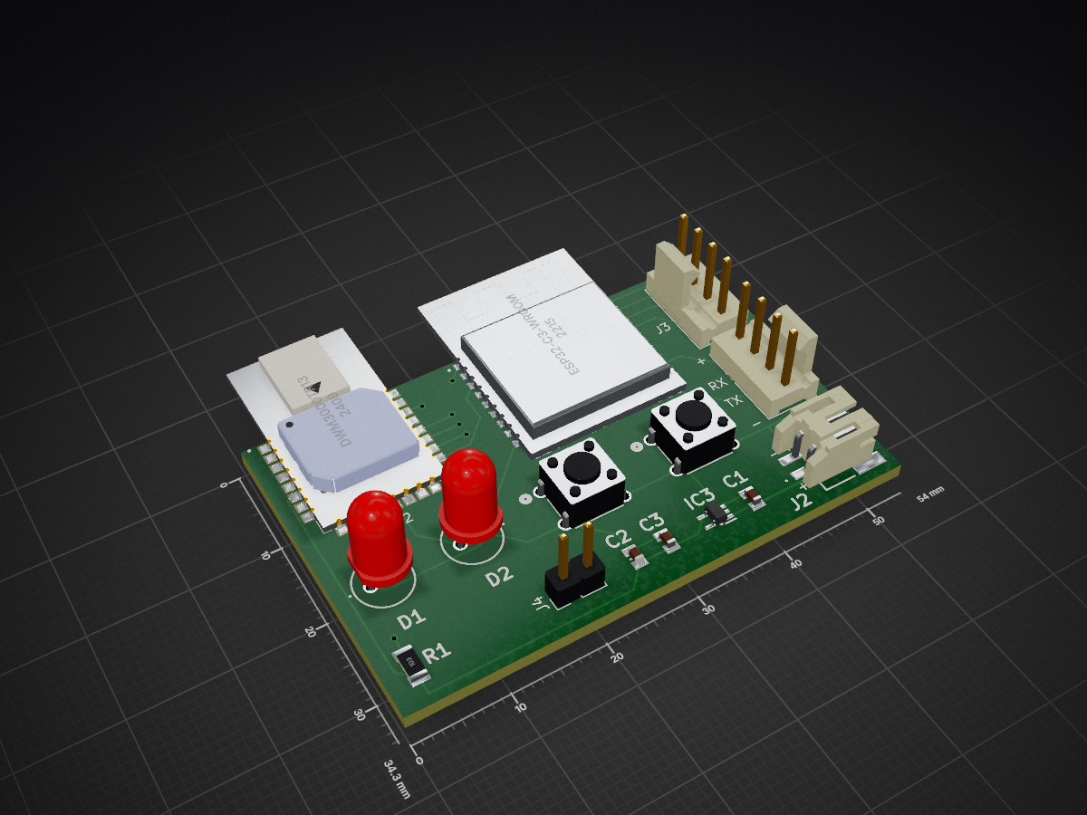
Pcb v2 is an open-source printed circuit board by hvtran21, from the hvtran21/SWAN repository on GitHub. It is a 2-layer board of 54 × 34.3 mm with 15 parts on 32 nets, routed with 169 tracks and 18 vias.
It is built around the DWM3000TR13, ESP32-C3-WROOM-02-N4 and TC1017-3.3VLTTR, with the TS02-66-50-BK-100-LCR-D among its other parts. Its parts include 4 connectors, 3 capacitors, 3 ICs, 2 diodes and 2 switches. It belongs with the ESP32 and RISC-V boards of this library.


SWAN (Secure Wireless Authentication Network) is a senior capstone project focused on developing a safer, more seamless alternative to traditional RFID and NFC-based access systems.
Current wireless access solutions, such as student ID cards or key fobs, suffer from two major issues:
SWAN leverages Ultra-Wideband (UWB) technology to deliver both stronger security and automatic, hands-free authentication.
Existing RFID and NFC access systems are vulnerable and inconvenient:
This is especially problematic in settings like dormitories or offices where secure yet convenient access is critical.
SWAN provides an automatic, secure, and user-friendly wireless authentication system powered by UWB.
Key design features:
The idea is that these tag devices can take space in your wallet as a card, and something on your keychain.
These are items that you typically always have on your person, and want to keep import track of. In the unfortunate event
that one of these devices are stolen, rest assured you're provided with a back biometric feature and that two tags
must be present at all times.
| Qty | Value | Footprint | References |
|---|---|---|---|
| 2 | 100nF | 100nF_footprint:CAPC2012X94N | C1, C3 |
| 2 | Conn_01x04_Pin | Connector:FanPinHeader_1x04_P2.54mm_Vertical | J1, J3 |
| 2 | LED | led_footprint:QED123A4R0 | D1, D2 |
| 2 | TS02-66-50-BK-100-LCR-D | 6mm_push_button_footprint:6mm_push_button_footprint | SW1, SW2 |
| 1 | 10K | 10k_ohm_footprint:RESC3216X65N | R1 |
| 1 | 10uF | 10uF_footprint:CAPC2012X140N | C2 |
| 1 | 1769 | lipo_charger_footprint:1769 | J2 |
| 1 | Conn_01x02_Pin | Connector_PinHeader_2.54mm:PinHeader_1x02_P2.54mm_Vertical | J4 |
| 1 | DWM3000TR13 | dwm3000_footprint:XCVR_DWM3000TR13 | IC2 |
| 1 | ESP32-C3-WROOM-02-N4 | esp_32_c3_footprint:ESP32C3WROOM02N4 | IC1 |
| 1 | TC1017-3.3VLTTR | footprint:SOT65P210X110-5N | IC3 |
hvtran21/SWAN
UMass Amherst ECE Senior Design Project - SWAN - A more secure and user centered solution to wireless access control.

hvtran21/SWAN
UMass Amherst ECE Senior Design Project - SWAN - A more secure and user centered solution to wireless access control.


davispe1/wearable-imu
Node PCB — revision 1.0. 4-layer board (F.Cu, In1.Cu, In2.Cu, B.Cu).

Harshul-Tripathi/asset-tracking-system
Industrial UWB tracking system and compact cell tag PCB, built with STMicroelectronics.

laemo10/SuperNicePCB
An integrated, multi-sensor UWB anchor PCB designed for real-time indoor object tracking (via Double-Sided Two-Way Ranging) and non-invasive human presence/occupancy monitoring.

mlumobi/uwm-indoor-localization-project
High precision indoor localization using Ultra Wide Band (UWB) technology.

tmb5932/fixed-wing-drone
The basics needed to allow a RC plane to be turned autonomous on signal.

It measures 54 × 34.3 mm and has 2 copper layers, 1.6 mm thick.
15 parts, built around the DWM3000TR13, ESP32-C3-WROOM-02-N4, TC1017-3.3VLTTR and TS02-66-50-BK-100-LCR-D. The full list of its parts is on this page, with links to each part's symbol and footprint where PCBKit's library has them.
From the hvtran21/SWAN repository on GitHub, at the commit this page was made from: the board is schematic_files/pcb_v2/pcb_v2.kicad_pcb and its schematic schematic_files/pcb_v2/pcb_v2.kicad_sch. PCBKit opens the board in the browser, with nothing to install.
Its repository states no licence, so its author keeps all rights: ask hvtran21 before reusing the design.