4 layers21.6 × 46.1 mm

 hlord2000/alpakka_pcb2
Alpakka is an open-source printed circuit board by hlord2000, from the hlord2000/alpakka_pcb repository on GitHub. It is a 4-layer board of 130 × 51 mm with 53 parts on 77 nets, routed with 576 tracks and 83 vias.
It is built around the PCAL6416AHF and LSM6DSL. Its parts include 20 switches, 8 capacitors, 6 ICs, 5 resistors and 5 connectors.


Alpakka controller Printed Circuit Board reference design
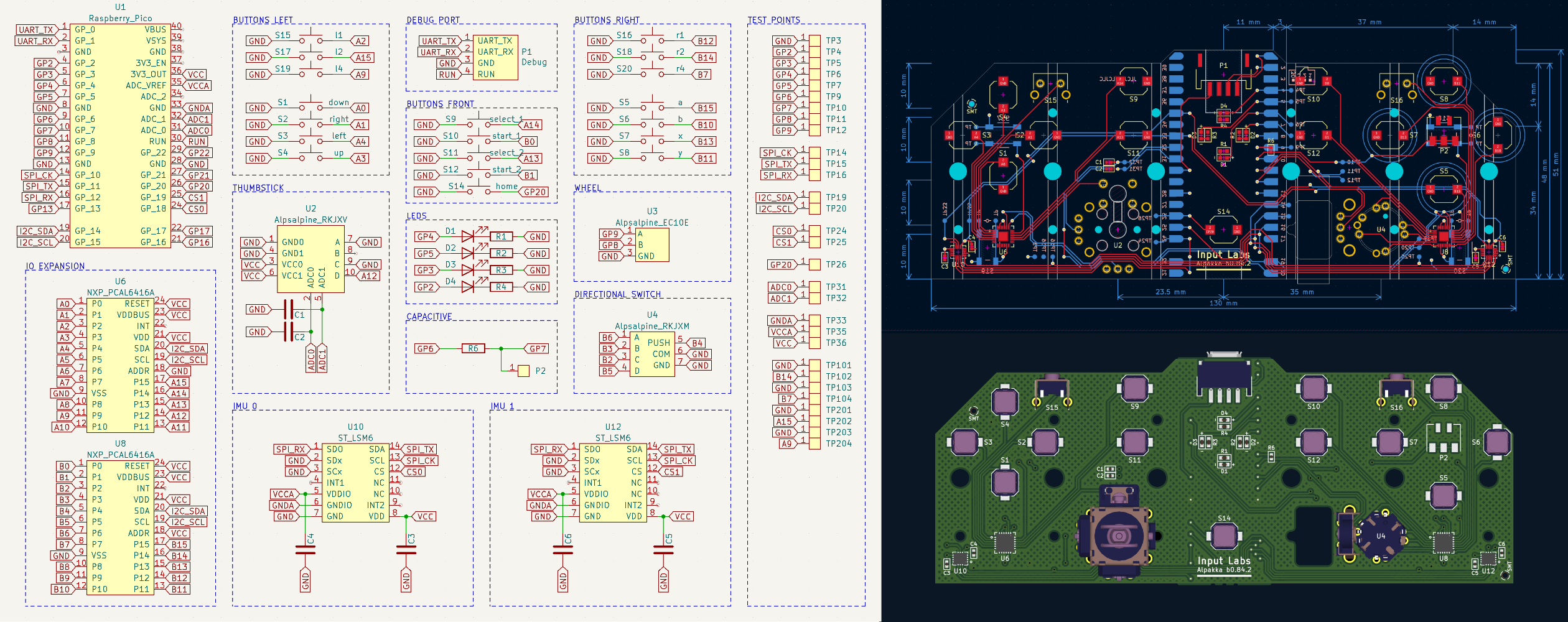
For ordering a reference design PCB (with no modifications) is possible to use the pre-built order files. Check the manual for step-by-step instructions.
.kicad_sch file in Schematics editor.Tools → Edit symbol fieldsGroupLCSC id for JLCPCB).plugins/kicad_ilo_export.py into KiCad plugins folder (PCB editor → menu Tools → External plugins → Reveal plugins folder)..kicad_pcb file in PCB editor.Edit → Fill all zonesTools → External plugins → Refresh pluginsTools → External plugins → Input Labs: exportorder/Preferences → Action pluginsConsolidated zones increase .kicad_pcb file size significantly, so instead is recommended to load and save the project without consolidation:
Edit → Fill all zones.Edit → Unfill all zones.| Qty | Value | Footprint | References |
|---|---|---|---|
| 4 | 100nF | Capacitor_SMD:C_0402_1005Metric | C9, C10, C11, C12 |
| 4 | 20 Ω | Resistor_SMD:R_0603_1608Metric | R1, R2, R3, R4 |
| 4 | 4.7uF | Capacitor_SMD:C_0603_1608Metric | C1, C2, C5, C6 |
| 4 | Diode | Diode_SMD:D_0603_1608Metric | D1, D2, D3, D4 |
| 3 | Endpoint | TestPoint:TestPoint_Pad_D1.0mm | TPP1, TPP2, TPP3 |
| 2 | Alpsalpine_RKJXV | ILO_fp:Alpsalpine_RKJXV122400R | U1, U2 |
| 2 | Conn_01x20_Pin | ILO_fp:Hirose_DF12NB_receptacle | P1, P2 |
| 2 | LOGO | LOGO | G***, G*** |
| 2 | LSM6DSL | Package_LGA:LGA-14_3x2.5mm_P0.5mm_LayoutBorder3x4y | U5, U6 |
| 2 | PCAL6416AHF | Package_DFN_QFN:HVQFN-24-1EP_4x4mm_P0.5mm_EP2.1x2.1mm | U3, U4 |
| 1 | 1 MΩ | Resistor_SMD:R_0402_1005Metric | R6 |
| 1 | A | ILO_fp:Alpsalpine_SKPM | S5 |
| 1 | B | ILO_fp:Alpsalpine_SKPM | S6 |
| 1 | Blade | ILO_fp:HRO_BC-25-3P | P4 |
| 1 | Conn_01x02 | Connector_JST:JST_PH_S2B-PH-K_1x02_P2.00mm_Horizontal | P6 |
| 1 | Conn_01x04 | ILO_fp:XKB_X6511FRS-04 | P3 |
| 1 | EC10E | ILO_fp:Alpsalpine_EC10E | SW1 |
| 1 | L1 | ILO_fp:Alpsalpine_SKHHL | S15 |
| 1 | L2 | ILO_fp:Alpsalpine_SKQG | S17 |
| 1 | L4 | ILO_fp:Alpsalpine_SKQG | S19 |
| 1 | R1 | ILO_fp:Alpsalpine_SKHHL | S16 |
| 1 | R2 | ILO_fp:Alpsalpine_SKQG | S18 |
| 1 | R4 | ILO_fp:Alpsalpine_SKQG | S20 |
| 1 | X | ILO_fp:Alpsalpine_SKPM | S7 |
| 1 | Y | ILO_fp:Alpsalpine_SKPM | S8 |
| 1 | down | ILO_fp:Alpsalpine_SKPM | S1 |
| 1 | home | ILO_fp:Alpsalpine_SKPM | S14 |
| 1 | left | ILO_fp:Alpsalpine_SKPM | S3 |
| 1 | right | ILO_fp:Alpsalpine_SKPM | S2 |
| 1 | select_1 | ILO_fp:Alpsalpine_SKPM | S9 |
| 1 | select_2 | ILO_fp:Alpsalpine_SKPM | S11 |
| 1 | start_1 | ILO_fp:Alpsalpine_SKPM | S10 |
| 1 | start_2 | ILO_fp:Alpsalpine_SKPM | S12 |
| 1 | up | ILO_fp:Alpsalpine_SKPM | S4 |

PyroVision-ThermalCam/Mainboard
Mainboard for the PyroVision thermal camera.


PyroVision-ThermalCam/Displayboard
Displayboard for the PyroVision thermal camera.


jlcjak/neurband
Open, minimal sEMG wristband like the Meta Neural Band: 8-ch ADS1298 + nRF52832 BLE, dry gold electrodes on a flex, 3D-printed band. KiCad, FreeCAD, Zephyr, Python, simulations.
It measures 130 × 51 mm and has 4 copper layers, 1.6 mm thick.
53 parts, built around the PCAL6416AHF and LSM6DSL. The full list of its parts is on this page, with links to each part's symbol and footprint where PCBKit's library has them.
From the hlord2000/alpakka_pcb repository on GitHub, at the commit this page was made from: the board is projects/alpakka/alpakka.kicad_pcb and its schematic projects/alpakka/alpakka.kicad_sch. PCBKit opens the board in the browser, with nothing to install.
Its repository states no licence, so its author keeps all rights: ask hlord2000 before reusing the design.