
4 layers234 × 84 mm
Main panel
google/mozc-devices
Circuit diagrams and firmware source code for Gboard DIY keyboards
234 parts3kApache-2.0
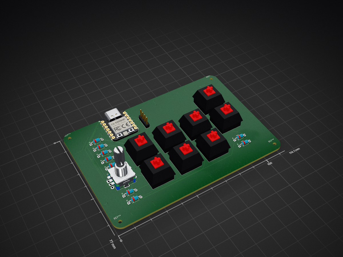
 hitenpanda/HackPad
This is a custom-made Advanced HackPad, which is coded to be used for your own services. It has a screen to help you monitor activities, it is customisable too. Also, has different menus but that is configured for me. You can make use of this project to create your own customised hackpad that is unique to you.
HackPad is an open-source printed circuit board by hitenpanda, from the hitenpanda/HackPad repository on GitHub. It is a 2-layer board of 114.1 × 77 mm with 40 parts on 45 nets, routed with 364 tracks and 49 vias.
It is built around the SK6812MINI-E. Its parts include 25 diodes, 9 switches, 1 IC and 1 connector. It belongs with the RP2040 boards of this library.
A custom parametric mechanical macropad powered by the Seeed Studio XIAO RP2040. Designed, routed in KiCad, and modeled in Fusion 360 for the Hack Club Blueprint initiative.
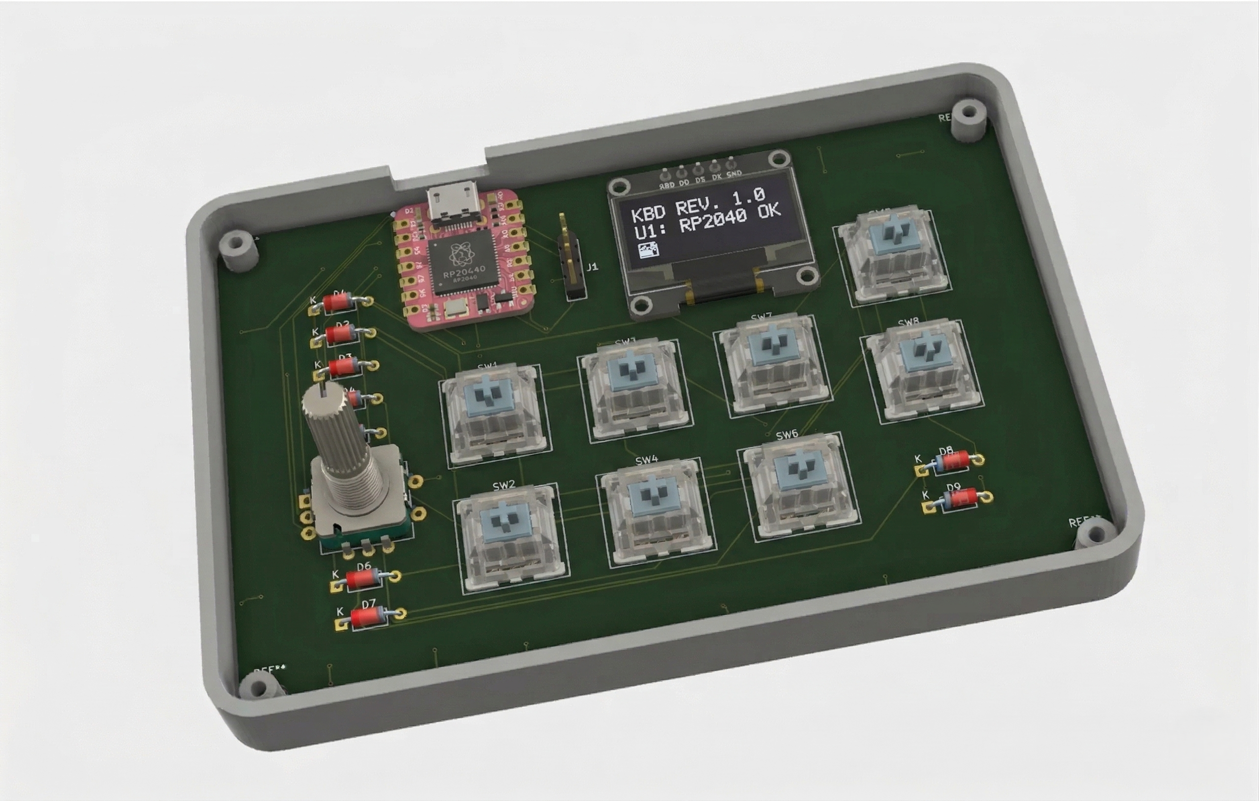
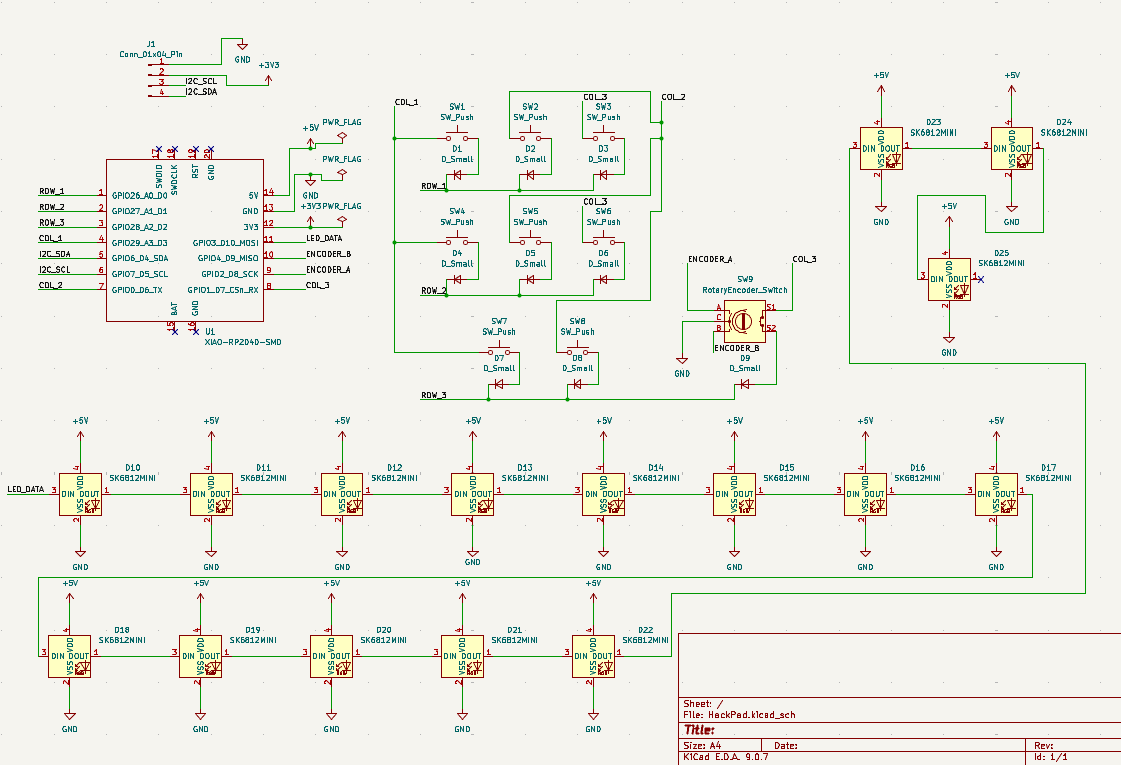
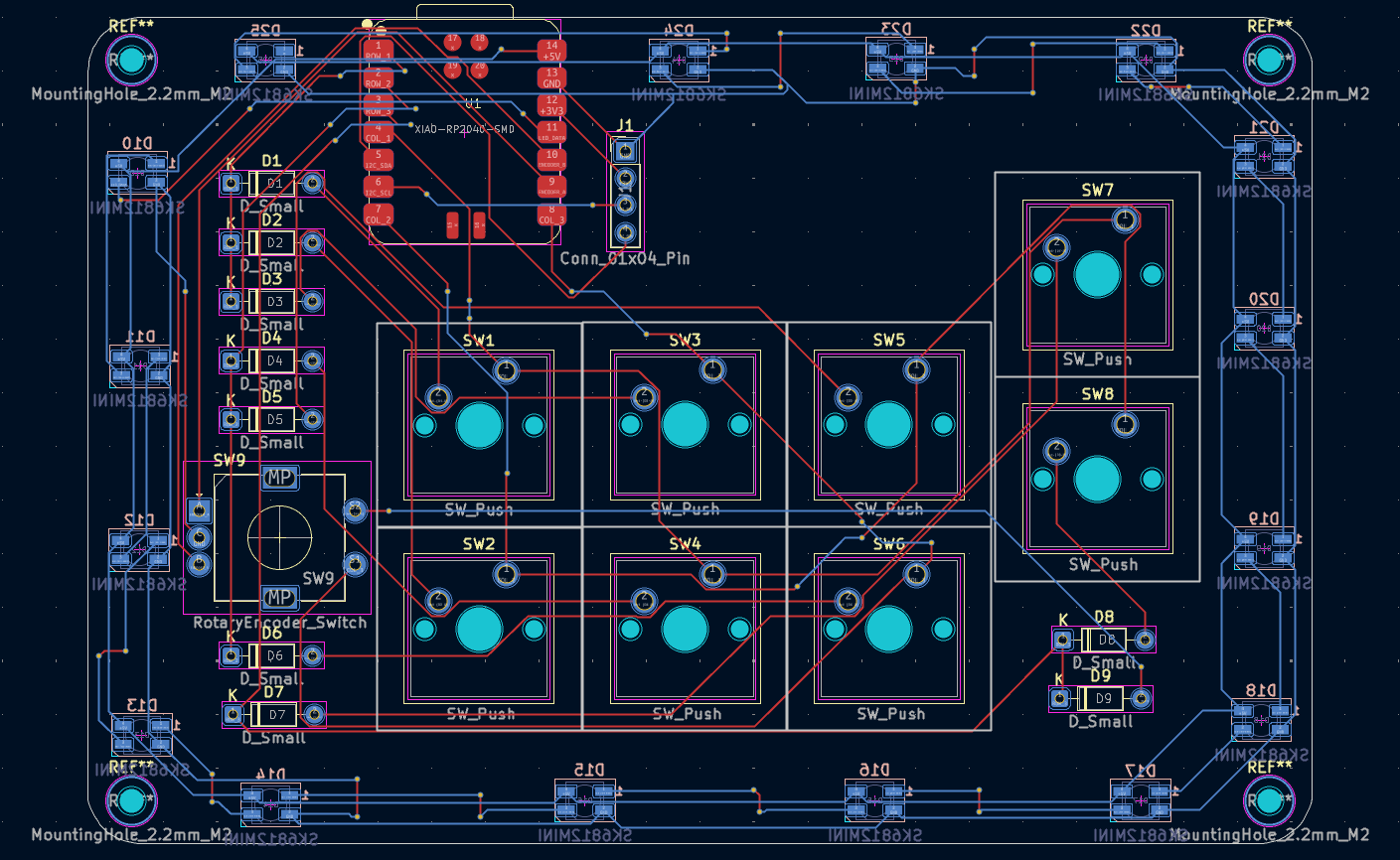
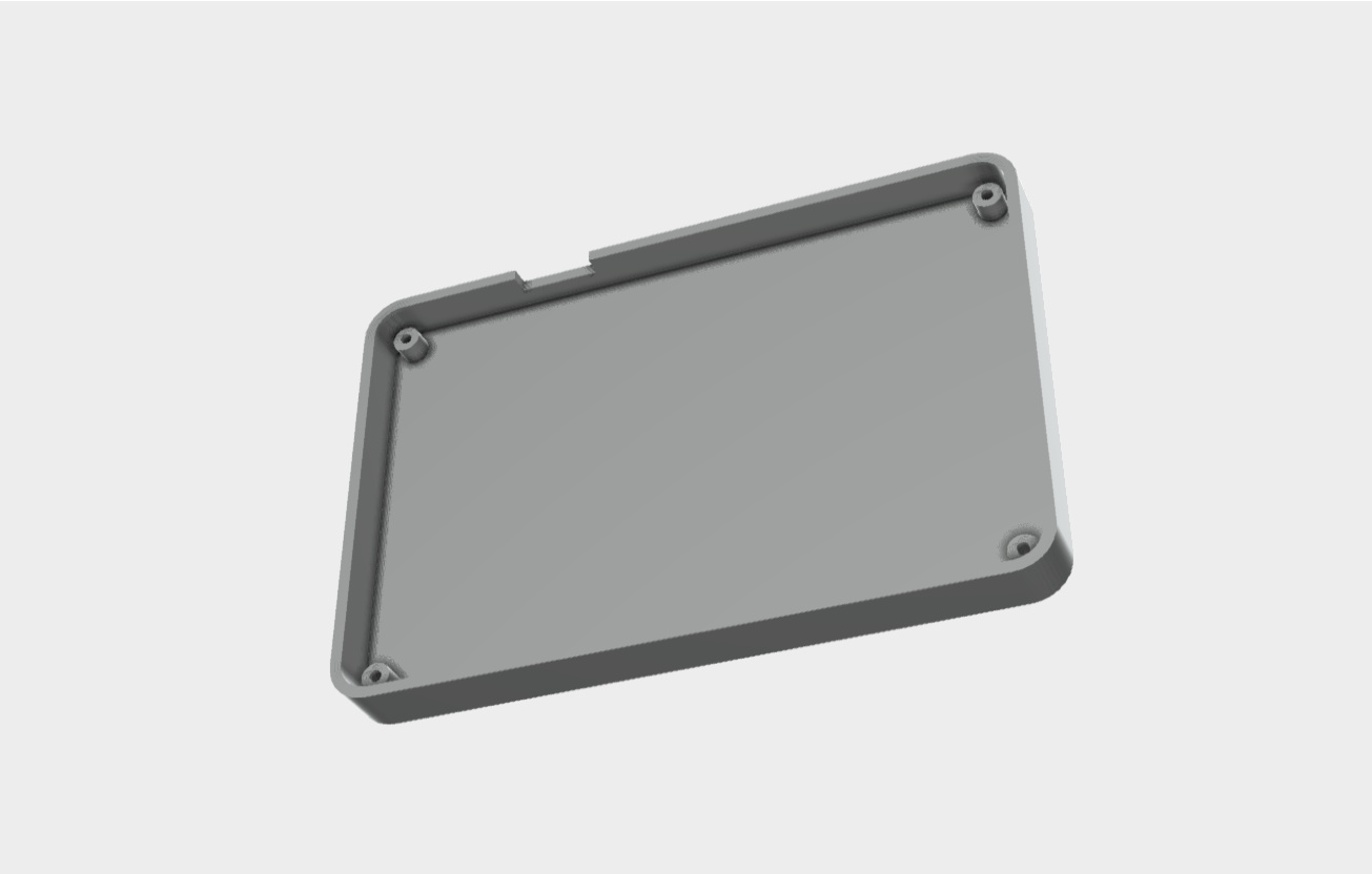 The enclosure is a parametric Lower Tray model built perfectly to fit the PCB outline. It uses a 2.0mm offset, 4.0mm standoffs, and 8.0mm walls for a clean "Floating Key" aesthetic.
| Part | Quantity | Description / Notes |
|---|---|---|
| Seeed Studio XIAO RP2040 | 1 | Main Microcontroller (Through-hole) |
| Mechanical Switches | 8 | Kailh Choc V2 switches |
| Keycaps | 8 | 1U Keycaps to fit each switch |
| Custom PCB | 1 | Custom 2-layer PCB |
| 3D Printed Tray (Bottom) | 1 | 2.0mm thick base with 8.0mm perimeter walls Translucent |
| Diodes | 9 | 1N4148 |
| Mounting Hardware | 4 | M2 2.2mm screws for securing PCB to tray standoffs and Heatset inserts |
| Display | 1 | 0.91" 128x32 OLED Display |
| Encoder | 1 | EC11 Rotary Encoder and 1 x 3D-Printed Knob |
To give reviewers insight into the design process, here is the technical breakdown of the hardware environment and enclosure architecture.
The current enclosure is modeled as a Lower Tray. The design logic is heavily parametric, ensuring that any future changes to the PCB automatically cascade into the 3D printed enclosure.
.step file. It serves as the absolute "Global Zero" for all sketch planes. All enclosure components are built on the underside of the board (Negative Z-axis) to ensure pin clearance.| Qty | Value | Footprint | References |
|---|---|---|---|
| 16 | SK6812MINI | LED_SMD:LED_SK6812MINI_PLCC4_3.5x3.5mm_P1.75mm | D10, D11, D12, D13, D14, D15, D16, D17, D18, D19, D20, D21, D22, D23, D24, D25 |
| 9 | D_Small | Diode_THT:D_DO-35_SOD27_P7.62mm_Horizontal | D1, D2, D3, D4, D5, D6, D7, D8, D9 |
| 8 | SW_Push | Button_Switch_Keyboard:SW_Cherry_MX_1.00u_PCB | SW1, SW2, SW3, SW4, SW5, SW6, SW7, SW8 |
| 1 | Conn_01x04_Pin | Connector_PinHeader_2.54mm:PinHeader_1x04_P2.54mm_Vertical | J1 |
| 1 | RotaryEncoder_Switch | Rotary_Encoder:RotaryEncoder_Alps_EC11E-Switch_Vertical_H20mm | SW9 |
| 1 | XIAO-RP2040-SMD | Seeed Studio XIAO Series Library:XIAO-RP2040-SMD | U1 |
The 36 most common of 40 parts.
It measures 114.1 × 77 mm and has 2 copper layers, 1.6 mm thick.
40 parts, built around the SK6812MINI-E. The full list of its parts is on this page, with links to each part's symbol and footprint where PCBKit's library has them.
From the hitenpanda/HackPad repository on GitHub, at the commit this page was made from: the board is PCB/HackPad.kicad_pcb and its schematic PCB/HackPad.kicad_sch. PCBKit opens the board in the browser, with nothing to install.
Its repository states no licence, so its author keeps all rights: ask hitenpanda before reusing the design.
google/mozc-devices
Circuit diagrams and firmware source code for Gboard DIY keyboards

Bastardkb/Dilemma
The Dilemma is a vertical stagger low-profile keyboard with mods.

Pwnsat/FlatSat
Flatsat v1.0 is a hardware based platform for aerospace cybersecurity research

adamws/kicad-kbplacer
KiCad plugin for automatic keyboard's key placement and routing

imchipwood/dumbpad
Simple 4x4 numpad with rotary encoder. Powered by QMK via ATmega32u4 Pro Micro

makerforgetech/modular-biped
An open source framework for creating a bipedal modular companion robot.

