2 layers100 × 100 mm

 Harshavar8jdm/BarelyScope
An Oscilloscope with very limited functionality
BarelyScope is an open-source printed circuit board by Harshavar8jdm, from the Harshavar8jdm/BarelyScope repository on GitHub. It is a 4-layer board of 90 × 80 mm with 36 parts on 56 nets, routed with 241 tracks and 54 vias.
It is built around the STM32L432KCU6, CONBNC001 and GSB1C41110SSHR. Its parts include 12 resistors, 9 capacitors, 4 connectors and 2 ICs. It belongs with the STM32 boards of this library.


BarelyScope is a compact, ultra-budget 2-channel digital oscilloscope based on the STM32F432CEU6 microcontroller. Designed within a compact 90 mm × 90 mm form factor, it features a built-in 1.8" color TFT display (ST7735R), dual BNC signal inputs, onboard controls, LED status indicators, and PC data streaming over USB.
| Top 3D Render | Bottom 3D Render |
|---|---|
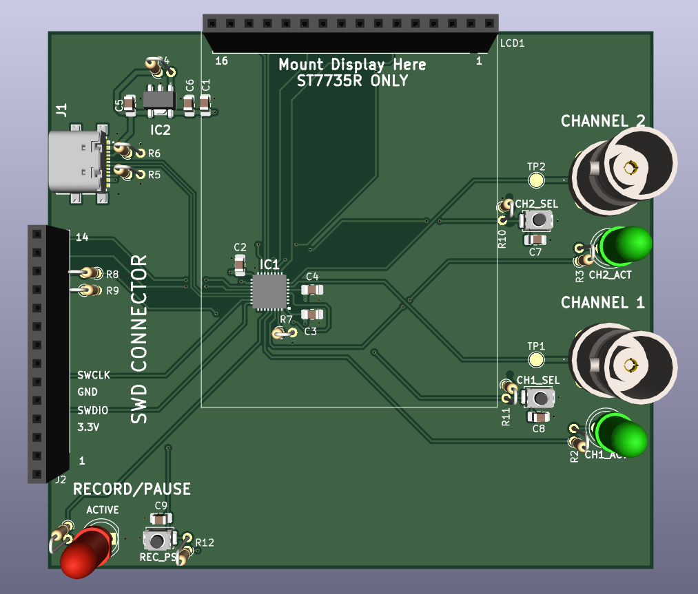 | 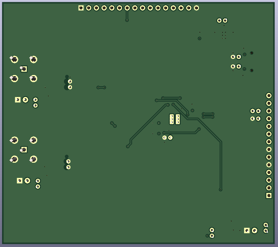 |
| PCB Layout | Circuit Schematic |
|---|---|
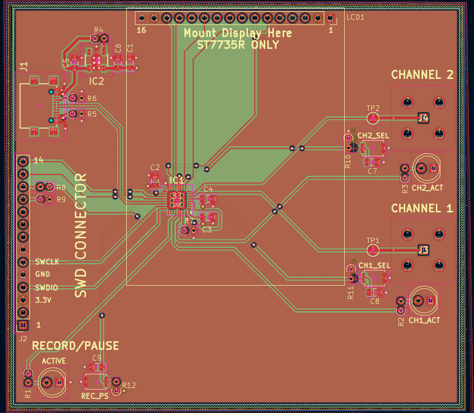 | 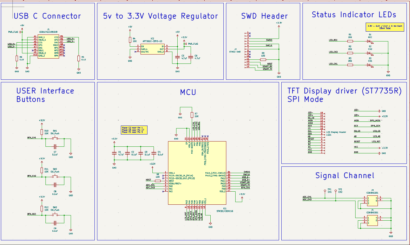 |
STM32L432KCU6 / STM32F432CEU6).CH1 and CH2) for probe hookup.0V to 3.3V native DC input range.BarelyScope utilizes a standard 4-layer PCB manufacturing stackup to ensure stable ground references and clean power distribution:
┌─────────────────────────────────────────────────────────────┐  Top Layer
│ Layer 1: Top Signal / High-Speed Traces & Components        │  (SIG)
├─────────────────────────────────────────────────────────────┤
│ Layer 2: Solid Ground Plane                                 │  (GND)
├─────────────────────────────────────────────────────────────┤
│ Layer 3: Power Rails (+3.3V)                                │  (PWR)
├─────────────────────────────────────────────────────────────┤
│ Layer 4: Bottom Signal / Secondary Ground Plane             │  (GND/SIG)
└─────────────────────────────────────────────────────────────┘ Bottom Layer| Parameter | Specification |
|---|---|
| Board Dimensions | 90 mm × 90 mm (3.54" × 3.54") |
| PCB Layers | 4 Layers (SIG - GND - PWR - GND) |
| Primary Voltage Regulator | AP7361C-33Y5-13 (5.0V to 3.3V LDO, SOT-89) |
| Input Interface | 2× BNC Connectors (J3, J4) |
| Display Interface | SPI Header for ST7735R 128×160 TFT Display |
| Debug / Flash Interface | Standard SWD Header (SWCLK, SWDIO, NRST, 3.3V, GND) |
| Power Input | USB Type-C (J1) |
While Revision 1.0 serves as an initial functional hardware prototype, several critical schematic and layout shortcomings were identified during design review. These items are tracked for correction in Revision 2.0:
PA0, PA1) without attenuation, current limiting, or ESD clamping. Voltages outside 0V–3.3V or static discharges will permanently damage the microcontroller.3.3V and GND (e.g., BAT54S).LED+) on the TFT header (LCD1) is tied directly to +3.3V without a current-limiting resistor, risking excessive current draw or LDO overload.VDDA / VREF+)VDDA/VREF+, Pin 5) shares the digital +3.3V power plane directly without LC/RC filtering, introducing digital switching noise into ADC measurements.VDDA from +3.3V via a ferrite bead and dedicated $100 ext{ nF} + 1\mu ext{F}$ decoupling capacitors placed directly adjacent to Pin 5.J2) uses a 14-pin pitch header, taking up excessive PCB real estate.J2 with a standard 5-pin $2.54 ext{ mm}$ single-row header (3.3V, SWDIO, SWCLK, GND, NRST) or a compact 6-pin Tag-Connect footprint.| Qty | Value | Footprint | References |
|---|---|---|---|
| 6 | 0.1uF | Capacitor_SMD:C_0805_2012Metric_Pad1.18x1.45mm_HandSolder | C2, C3, C4, C7, C8, C9 |
| 6 | 10K | Resistor_THT:R_Axial_DIN0204_L3.6mm_D1.6mm_P1.90mm_Vertical | R4, R7, R8, R10, R11, R12 |
| 3 | 200 | Resistor_THT:R_Axial_DIN0204_L3.6mm_D1.6mm_P1.90mm_Vertical | R1, R2, R3 |
| 3 | 4.7uF | Capacitor_SMD:C_0805_2012Metric_Pad1.18x1.45mm_HandSolder | C1, C5, C6 |
| 3 | SW_Push | Button_Switch_SMD:SW_Push_SPST_NO_Alps_SKRK | CH1_SEL, CH2_SEL, REC_PS |
| 2 | 5.1K | Resistor_THT:R_Axial_DIN0204_L3.6mm_D1.6mm_P1.90mm_Vertical | R5, R6 |
| 2 | CONBNC001 | BNC Connector:CONBNC001 | J3, J4 |
| 1 | 100 | Resistor_THT:R_Axial_DIN0204_L3.6mm_D1.6mm_P1.90mm_Vertical | R9 |
| 1 | AP7361C-33Y5-13 | AP7361-33Y5-13:AP7361CY513 | IC2 |
| 1 | CH1 | TestPoint:TestPoint_Pad_D2.0mm | TP1 |
| 1 | CH1 | LED_THT:LED_D5.0mm | CH2_ACT |
| 1 | CH2 | LED_THT:LED_D5.0mm | CH1_ACT |
| 1 | CH2 | TestPoint:TestPoint_Pad_D2.0mm | TP2 |
| 1 | GSB1C41110SSHR | GSB1C41110SSHR:GSB1C41110SSHR | J1 |
| 1 | LCD Display Header | Connector_PinSocket_2.54mm:PinSocket_1x16_P2.54mm_Vertical | LCD1 |
| 1 | REC | LED_THT:LED_D5.0mm | ACTIVE |
| 1 | STM32 SWD | Connector_PinSocket_2.54mm:PinSocket_1x14_P2.54mm_Vertical | J2 |
| 1 | STM32L432KCU6 | STM32L432KCU6:QFN50P500X500X60-33N-D | IC1 |
It measures 90 × 80 mm and has 4 copper layers, 1.6 mm thick.
36 parts, built around the STM32L432KCU6, CONBNC001 and GSB1C41110SSHR. The full list of its parts is on this page, with links to each part's symbol and footprint where PCBKit's library has them.
From the Harshavar8jdm/BarelyScope repository on GitHub, at the commit this page was made from: the board is BarelyScope.kicad_pcb and its schematic BarelyScope.kicad_sch. PCBKit opens the board in the browser, with nothing to install.
Its repository states no licence, so its author keeps all rights: ask Harshavar8jdm before reusing the design.


HarveyBates/Open-JIP
An open-source Arduino based chlorophyll fluorometer for quantifying photosynthesis in photosynthetic organisms.


borkdlabs/hoppy_clock
STM32-based alarm clock and RGB lamp: custom alarms wake you with light and your own songs, configured over USB from the browser or a Python tool


B-Leadr/STM32L4KC-Development-Board
A custom made mini development board for the STM32L432KC6 low power MCU.
