4 layers49.1 × 54.3 mm
Rp2350-hdmi hexpansion
Corteil/rp2350-hdmi-hexpansion
RP2350 HDMI hexpansion for the EMF Tildagon badge -- mirrors the badge's display to a monitor over HSTX/DVI
57 parts2
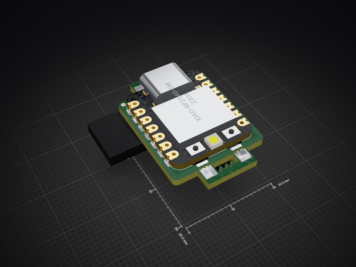
 HalFrgrd/slickbug
A small SWD programmer using the Seeed Studio XIAO RP2040. I wanted a compact debugger with a tiny target footprint (roughly 4.8mm by 1.1mm).
Slickbug is an open-source printed circuit board by HalFrgrd, from the HalFrgrd/slickbug repository on GitHub, published under the MIT licence. It is a 2-layer board of 20.3 × 30.3 mm with 10 parts on 19 nets, routed with 67 tracks and 11 vias.
It is built around the MAX40203AUK+T and JK-SMD0805-020-30V. Its parts include 4 ICs, 2 resistors, 2 connectors, 1 capacitor and 1 fuse. It belongs with the interfaces and adapters boards and the RP2040 boards of this library.


A small SWD programmer using the Seeed Studio XIAO RP2040. I wanted a compact debugger with a tiny target footprint (roughly 4.8mm by 1.1mm).
It uses four R50 test probe receptacles which are mounted on the back of the PCB and are held in place using two PCB "combs". P50 test probes sit in the R50 receptacles. The GND pin extends 1.5mm further so that GND connects first.
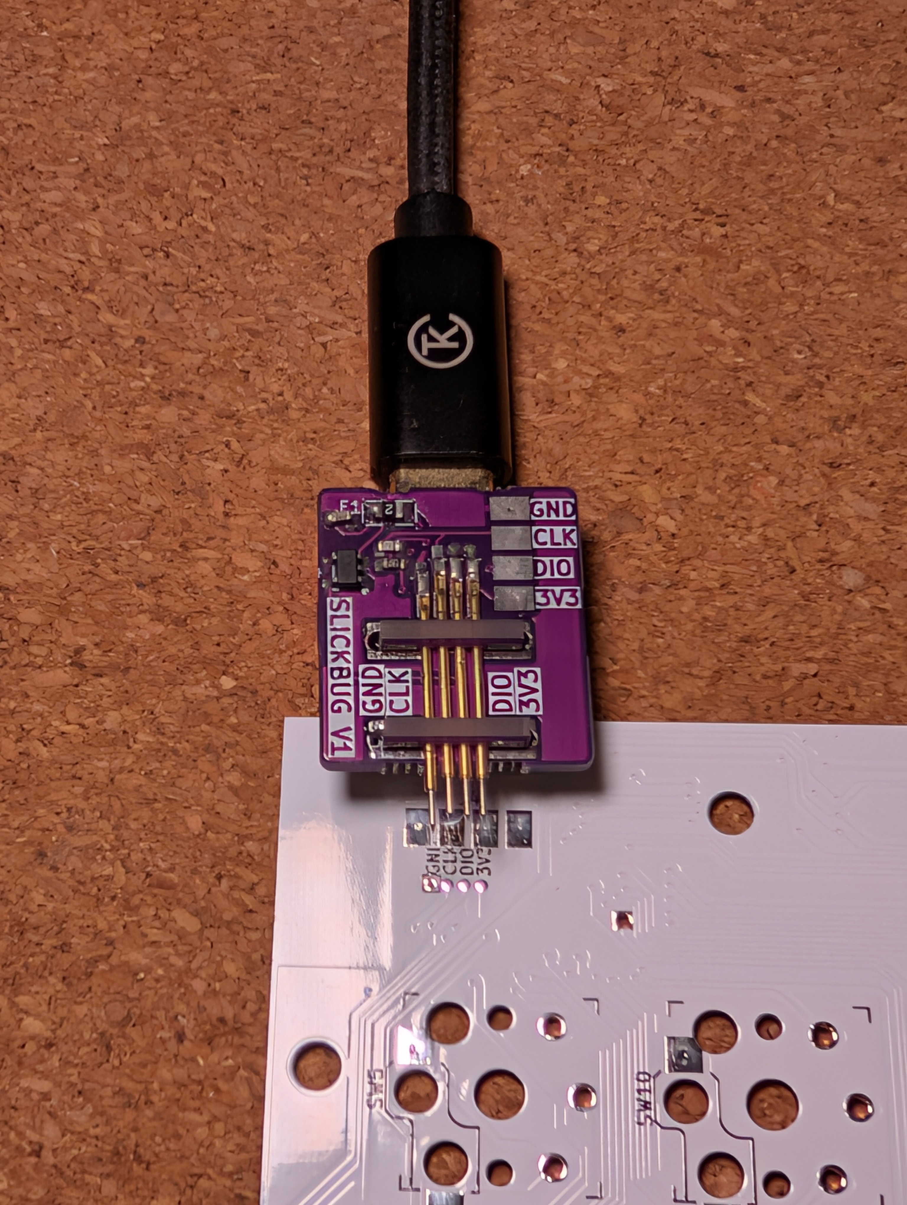
The target footprint is 4 pads with pitch 1.27mm:
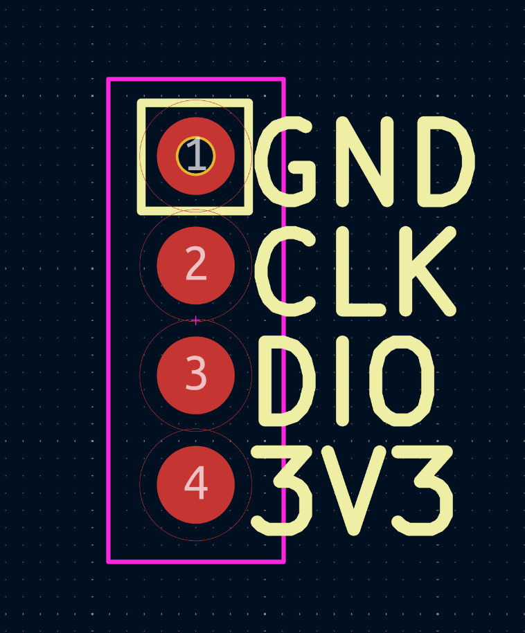 | 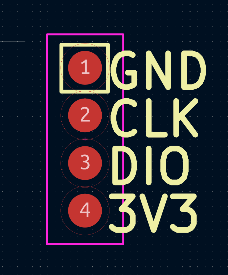 | 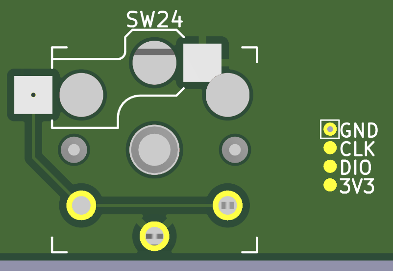 |
|---|---|---|
| PCB footprint with guiding hole | PCB footprint SMD only | Target footprint next to a MX keyswitch |
A standalone KiCad library containing only the target symbol and footprint is located in hardware/slick_bug_target/
Add it to your KiCad project with:
hardware/slick_bug_target/ into your project (or add this repo as a submodule).Footprint Library: Go to Preferences->Manage Footprint Libraries, click the folder icon, and select hardware/slick_bug_target/slick_bug_target.prettySymbol Library: Go to Preferences->Manage Symbol Libraries, add hardware/slick_bug_target/slick_bug_target.kicad_symslick_bug_target:Conn_SWD_SlickBug_V1 in your schematic. It already has slick_bug_target:SlickBug_Target_V1 pre-assigned as its footprint.Drag the production files to JLCPCB's order page to get the PCBs. 1.6mm thick so that the combs work as intended.
You can get the components from LCSC and combine your order with JLCPCB. I bought the test probes and receptacles from AliExpress.
You will need to snap off the combs from the pcb to hold the R50 receptacles in place.
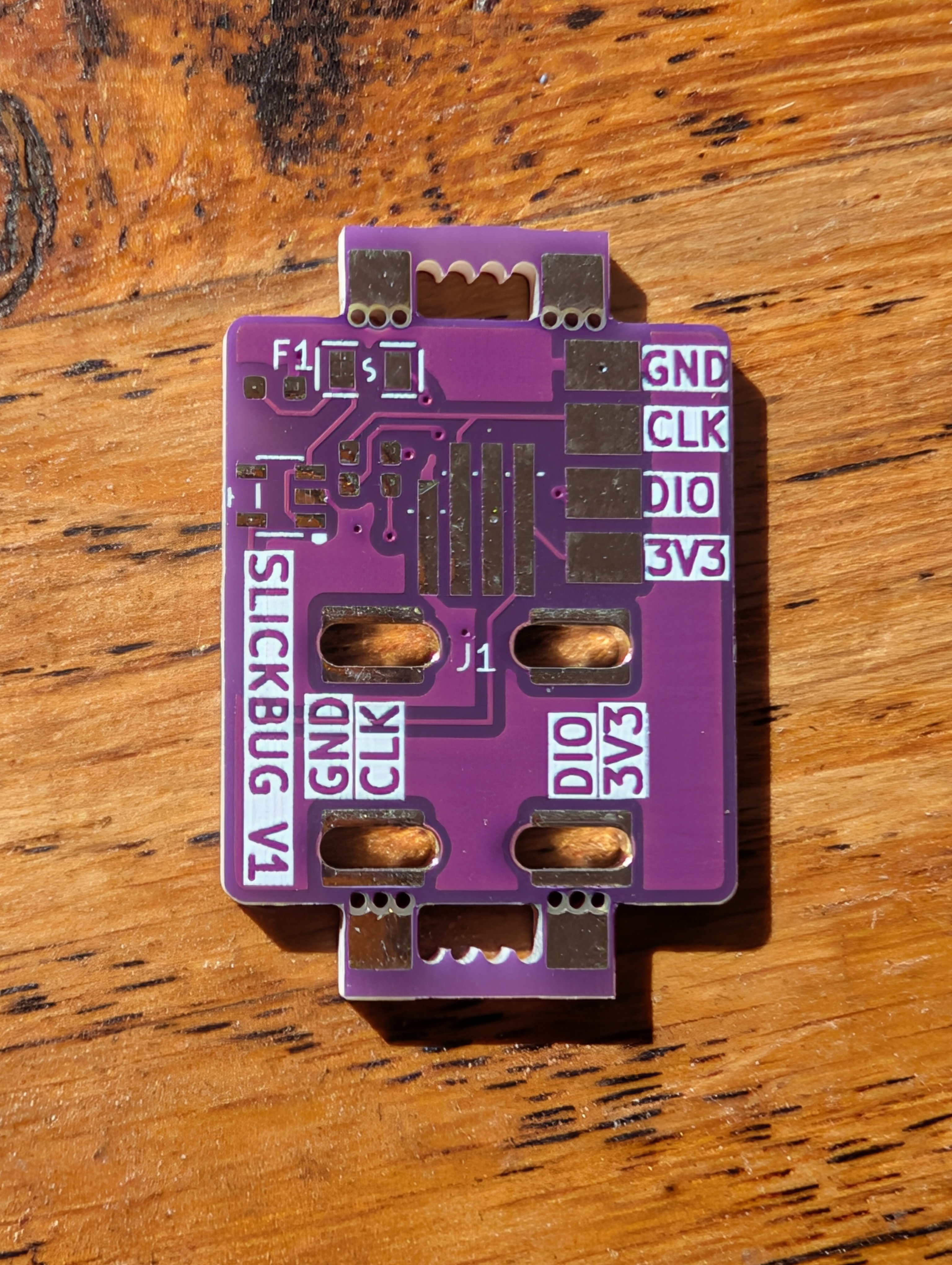 | 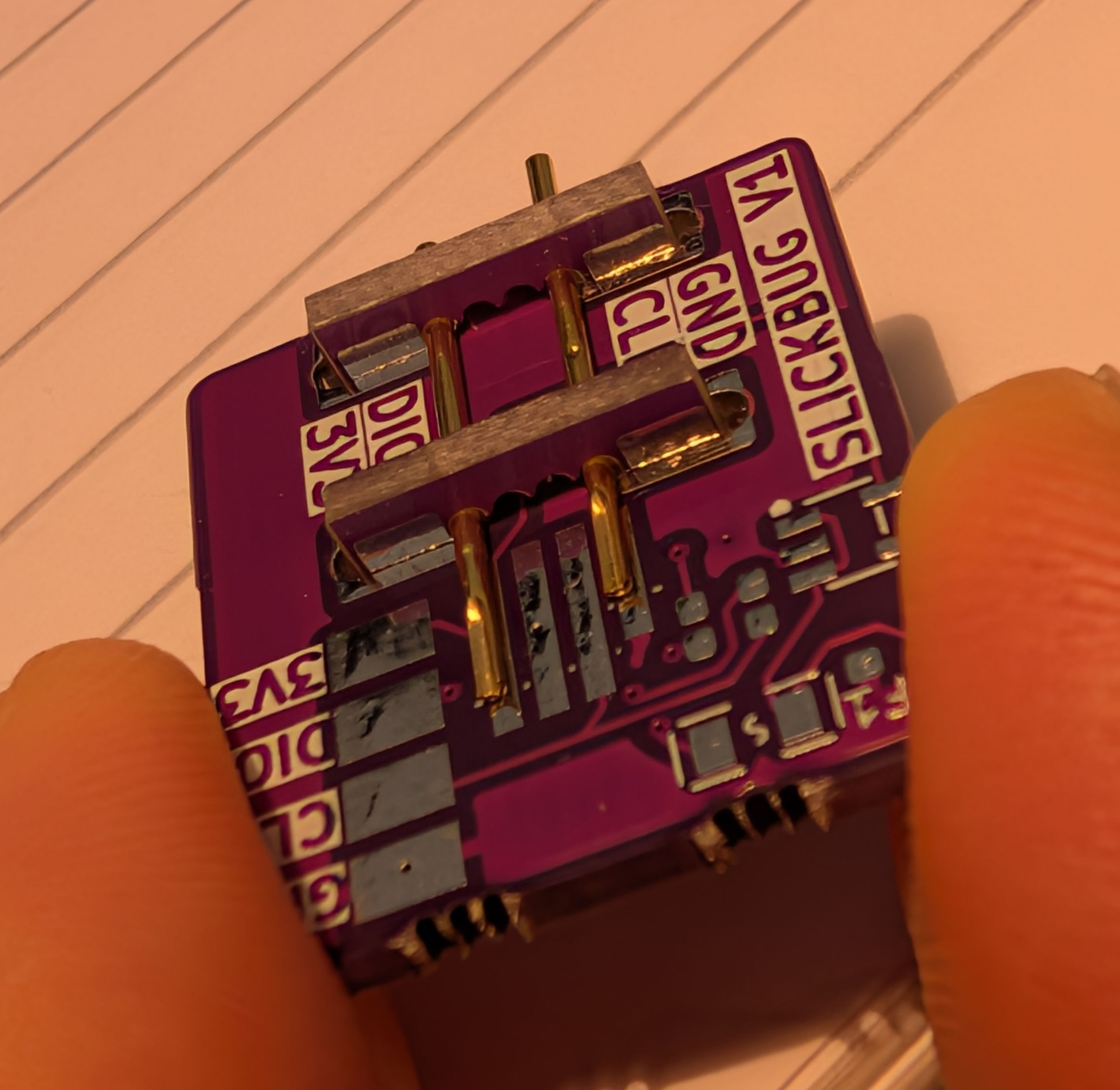 |
|---|---|
| SlickBug PCB | Partly assembled |
SlickBug uses the same SWD GPIO pins (GPIO 2 = SWCLK, GPIO 3 = SWDIO) as a Raspberry Pi Pico, so it runs the unmodified official debugprobe_on_pico.uf2 firmware (also included in firmware/debugprobe_on_pico.uf2):
B, tap R, release B).firmware/debugprobe_on_pico.uf2 onto the RPI-RP2 drive.| Qty | Value | Footprint | References |
|---|---|---|---|
| 2 | 33Ω | PCM_JLCPCB:R_0603 | R1, R2 |
| 2 | ~ | slick_bug:R50_pcb_comb | U2, U3 |
| 1 | 1uF | PCM_JLCPCB:C_0603 | C1 |
| 1 | Conn_01x04_Socket | slick_bug:Harwin_M20-89004xx_1x04_P2.54mm_Horizontal_blank | J2 |
| 1 | Conn_01x04_Socket | slick_bug:R50_horizontal_4pin | J1 |
| 1 | JK-SMD0805-020-30V | slick_bug:F0805 | F1 |
| 1 | MAX40203AUK+T | slick_bug:SOT-23-5_L3.0-W1.6-P0.95-LS2.8-BR | U4 |
| 1 | XIAO-RP2040-SMD | slick_bug:XIAO-RP2040-SMD | U1 |
It measures 20.3 × 30.3 mm and has 2 copper layers, 1.6 mm thick.
10 parts, built around the MAX40203AUK+T and JK-SMD0805-020-30V. The full list of its parts is on this page, with links to each part's symbol and footprint where PCBKit's library has them.
From the HalFrgrd/slickbug repository on GitHub, at the commit this page was made from: the board is hardware/slick_bug.kicad_pcb and its schematic hardware/slick_bug.kicad_sch. PCBKit opens the board in the browser, with nothing to install.
Its repository publishes it under the MIT licence: you may reuse it on that licence's terms (keep the author's notice, and for a copyleft licence share your changes alike).
Corteil/rp2350-hdmi-hexpansion
RP2350 HDMI hexpansion for the EMF Tildagon badge -- mirrors the badge's display to a monitor over HSTX/DVI

Ismael034/usbsp
Have you ever tried to plug a USB device into a computer that has USB restrictions enabled? It's frustrating, isn't it? You can't use your USB devices, and you have no way to bypass the restrictions.


Arrow-air/project-caribou
Project Caribou documentation, designs, and project artifacts.


calcpsu/cphp82001
CalcPack replacement for HP 82001, suits HP35/45/55/65/67 calculators
