2 layers49.6 × 52.8 mm
ICE40UP5K logic analyzer
hack-a-tack/FPGA_Logic_Analyzer
(Info applies to rev. 1, update for later revisions (only final rev. matters in the README)) FPGA-based 8-channel logic analyzer implemented on iCE40UP5K.
80 parts
 hack-a-tack/FPGA_Logic_Analyzer
(Info applies to rev. 1, update for later revisions (only final rev. matters in the README)) FPGA-based 8-channel logic analyzer implemented on iCE40UP5K.
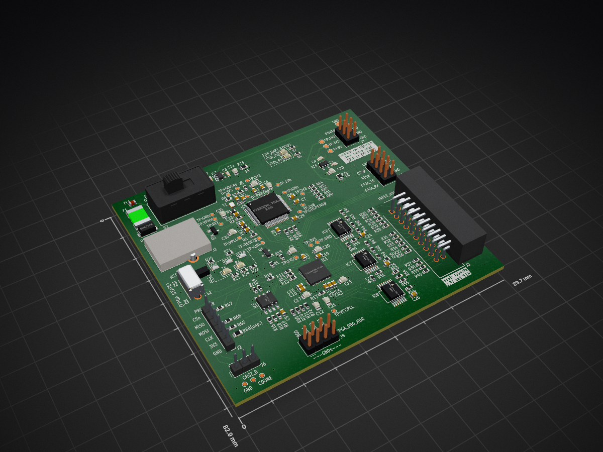
ICE40UP5K logic analyzer rev2 is an open-source printed circuit board by hack-a-tack, from the hack-a-tack/FPGA_Logic_Analyzer repository on GitHub. It is a 4-layer board of 89.7 × 82.9 mm with 170 parts on 153 nets, routed with 1,028 tracks and 202 vias.
It is built around the ICE40UP5K-SG48I, FT2232HL-TRAY and W25Q40CLSNIG, with the SN74LVC14ADBRE4, MIC5504-1.2YM5-TR and MIC5504-3.3YM5-TR among its other parts. Its parts include 74 resistors, 38 capacitors, 9 diodes, 8 ICs and 7 connectors. It belongs with the sensors and measurement boards and the FPGA and CPLD boards of this library.


(NOTE TO SELF: THIS MUST BE UPDATED FOR THE FINAL REVISION; REV1 IS VIRTUALLY IRRELEVANT HERE, ONLY RELEVANT IN REPORT IF USED TO DISCUSS IMPORTANT DESIGN DECISIONS)
(Info applies to rev. 1, update for later revisions (only final rev. matters in the README)) FPGA-based 8-channel logic analyzer implemented on iCE40UP5K. Supports 24 MHz sampling, 4096 sample depth, UART streaming and trigger logic.
Key specs:
| Spec | Value |
|---|---|
| FPGA | iCE40UP5K |
| Sampling channels | 8 |
| Sampling rate | 24MHz |
| Buffer | 4096 samples |
| Interface | UART |
| Programming | SPI |
| PCB | 2-layer |
| Revision | 1. |
// Note to self: block diagram, + explain modules briefly (less than a full sentence for each)
(insert block diagram)
(module overview:)
| Module | Description |
|---|---|
| capture_engine.vhd | samples digital inputs |
| analyzer_fsm.vhd | manages logic analyzer state |
| send_engine.vhd | UART streaming of captured data |
| ... | ... |
(table of performance metrics)
| Metric | Value |
|---|---|
| Sample rate | 24MHz |
| Buffer depth | 4096 samples |
| UART throughput | 3Mbaud |
| Capture latency | 3 cycles |
| LUT usage | 1420 |
| BRAM usage | 4 |
(Brief instructions)
For a more in-depth overview, check out the project report (add github route and link).
| Qty | Value | Footprint | References |
|---|---|---|---|
| 22 | 0u1 | 0u1_0603_cap_C0603C104M4RAC:CAPC1608X95N | C10, C11, C13, C14, C16, C18, C19, C24, C25, C26, C27, C28, C29, C30, C31, C32 +6 |
| 17 | 100k | Resistor_SMD:R_0603_1608Metric | R16, R41, R42, R43, R44, R45, R46, R47, R48, R49, R50, R51, R52, R53, R54, R55 +1 |
| 17 | 330R | Resistor_SMD:R_0603_1608Metric | R21, R25, R26, R27, R28, R29, R30, R31, R32, R33, R34, R35, R36, R37, R38, R39 +1 |
| 16 | 10k | Resistor_SMD:R_0603_1608Metric | R1, R3, R8, R9, R10, R15, R18, R19, R57, R58, R59, R60, R61, R62, R63, R64 |
| 11 | 4u7 | 4u7_0805_cap_C0805C475K4RACTM:C0805 | C1, C12, C15, C17, C20, C21, C22, C23, C34, C35, C38 |
| 9 | 100R | Resistor_SMD:R_0603_1608Metric | R14, R17, R65, R66, R67, R69, R70, R71, R72 |
| 6 | 680R | Resistor_SMD:R_0603_1608Metric | R6, R7, R20, R22, R23, R24 |
| 4 | 1u | 1u_0603_cap_MBASE168SB7105KTNA18:INDC1608X90N | C2, C3, C4, C5 |
| 4 | GND | TestPoint:TestPoint_Pad_D1.0mm | TP:GND, TP:GND, TP13, TP14 |
| 3 | 0R | Resistor_SMD:R_0805_2012Metric | R68, R73, R74 |
| 3 | 22R | Resistor_SMD:R_0603_1608Metric | R11, R12, R13 |
| 3 | SN74LVC14ADBRE4 | Schmitt_trigger_buffer_SN74LVC14ADBRE4:SOP65P780X200-14N | IC6, IC7, IC8 |
| 2 | 61300821121 | 8pin_header_2x4_61300821121:J_Wurth_WR-PHD_61300821121 | J4, J5 |
| 2 | BLM18AG601SN1D | Ferrite_bead_BLM18AG601SN1D:BLM18SP221SN1B | FB1, FB2 |
| 1 | 12k | Resistor_SMD:R_0603_1608Metric | R2 |
| 1 | 1V2 | TestPoint:TestPoint_Pad_D1.5mm | TP3 |
| 1 | 1k | Resistor_SMD:R_0603_1608Metric | R5 |
| 1 | 2920L050_72DR | Polyfuse_2920L050_72DR:FUSC7451X125N | F1 |
| 1 | 2N7002H6327XTSA2 | NMOS_2N7002H6327XTSA2:SOT95P240X110-3N | Q1 |
| 1 | 3V3 | TestPoint:TestPoint_Pad_D1.5mm | TP2 |
| 1 | 3u3 | 4u7_0805_cap_C0805C475K4RACTM:C0805 | C6 |
| 1 | 4k7 | Resistor_SMD:R_0603_1608Metric | R4 |
| 1 | 5V | TestPoint:TestPoint_Pad_D1.5mm | TP1 |
| 1 | 61202021621 | 20_pin_2x10_shrouded_header_61202021621:SHDR20W64P254_2X10_3306X910X885P | J3 |
| 1 | 61300311121 | 8pin_header_2x4_61300821121:J_Wurth_WR-PHD_61300311121 | J6 |
| 1 | 61300611121 | 6_pin_header_61300611121:HDRV6W64P0X254_1X6_1524X254X869P | J2 |
| 1 | 61300621121 | 6pin_header_2x3_61300621121:J_Wurth_WR-PHD_61300621121 | J7 |
| 1 | 830208214809 | 12MHz_CMOS_clock_830208214809:830208214809 | Y1 |
| 1 | BLM21SP601SN1D | Ferrite_bead_BLM21SP601SN1D:BLM21AG102BH1J | FL1 |
| 1 | CDONE | TestPoint:TestPoint_Pad_D1.0mm | TP5 |
| 1 | CRESET_B | TestPoint:TestPoint_Pad_D1.0mm | TP6 |
| 1 | DONE | Green_LED_0805_150060VS75003:150060VS75003 | D4 |
| 1 | FT2232HL-TRAY | UART_USB_bridge_FT2232HL:QFP50P1200X1200X160-64N | IC4 |
| 1 | FTDI_RX | Blue_LED_0805_APT2012LVBC/D:LEDC2012X85N | D8 |
| 1 | FTDI_TX | Yellow_LED_0805_150080YS75000:LEDC2012X70N | D9 |
| 1 | FTDI_VCCIO | TestPoint:TestPoint_Pad_D1.0mm | TP:3V3 |
| 1 | FTDI_VCORE | TestPoint:TestPoint_Pad_D1.0mm | TP:1V8 |
| 1 | FTDI_VREGIN | TestPoint:TestPoint_Pad_D1.0mm | TP:3V3 |
| 1 | GND | TestPoint:TestPoint_Pad_D1.5mm | TP4 |
| 1 | ICE40UP5K-SG48I | ICE40UP5K-SG48I:QFN50P700X700X100-49N-D | IC1 |
| 1 | L101011MS02Q | Slide_switch_SPST_ON/OFF_L101011MS02Q:L101011MS02Q | S2 |
| 1 | MIC5504-1.2YM5-TR | MIC5504-1.2YM5-TR:SOT95P280X145-5N | IC3 |
| 1 | MIC5504-3.3YM5-TR | MIC5504-3.3YM5-TR:SOT95P280X145-5N | IC2 |
| 1 | OS102011MA1QN1 | Slide_switch_SPDT_ON/ON_OS102011MA1QN1:OS102011MA1QN1 | S1 |
| 1 | PWR | Green_LED_0805_150060VS75003:150060VS75003 | D3 |
| 1 | PWREN# | TestPoint:TestPoint_Pad_D1.0mm | TP:PWREN# |
| 1 | PWRSAV# | TestPoint:TestPoint_Pad_D1.0mm | TP:PWRSAV |
| 1 | REF | TestPoint:TestPoint_Pad_D1.0mm | TP:REF |
| 1 | RESET# | TestPoint:TestPoint_Pad_D1.0mm | TP:RESET# |
| 1 | RX | Blue_LED_0805_APT2012LVBC/D:LEDC2012X85N | D7 |
| 1 | SMAJ5.0A | TVS_diode_SMAJ5_0A:DIOM5127X229N | D1 |
| 1 | SP0502BAHTG | ESD_diode_array_3pin_SP0502BAHTG:SOT95P237X112-3N | D2 |
| 1 | SUSPEND# | TestPoint:TestPoint_Pad_D1.0mm | TP:SUSPEND# |
| 1 | TEST | TestPoint:TestPoint_Pad_D1.0mm | TP:GND |
| 1 | TX | Yellow_LED_0805_150080YS75000:LEDC2012X70N | D6 |
| 1 | USB B Female Connector | USB_B_Female_Connector:61400416121 | J1 |
| 1 | USER | White_LED_0805_150060WS75000:150060WS75000 | D5 |
| 1 | VCC | TestPoint:TestPoint_Pad_D1.0mm | TP:1V2 |
| 1 | VCCIO | TestPoint:TestPoint_Pad_D1.0mm | TP:3V3 |
| 1 | VCC_PLL | TestPoint:TestPoint_Pad_D1.0mm | TP:VCCPLL |
| 1 | VPHY | TestPoint:TestPoint_Pad_D1.0mm | TP:VPHY |
| 1 | VPLL | TestPoint:TestPoint_Pad_D1.0mm | TP:VPLL |
| 1 | VREGOUT | TestPoint:TestPoint_Pad_D1.0mm | TP:1V8 |
| 1 | VS_OSC | TestPoint:TestPoint_Pad_D1.0mm | TP:3V3 |
| 1 | W25Q40CLSNIG | SPI_flash_NOR_W25Q40CLSNIG:SOIC127P600X175-8N | IC5 |
hack-a-tack/FPGA_Logic_Analyzer
(Info applies to rev. 1, update for later revisions (only final rev. matters in the README)) FPGA-based 8-channel logic analyzer implemented on iCE40UP5K.

c0pperdragon/A-VideoBoard
FPGA board to create a component video signal for vintage computers.

Acliad/Nifty-Numpad
Full sized numpad with an extra row and two extra columns of macro keys. It was created as a companion to my TKL keyboard for CAD design.

Acliad/XBOX-Sign
A "weekend" project converting a vanity Xbox sign to the OG Xbox style

MicroCoreLabs/Projects
Ted Fried's MicroCore Labs Projects - FPGA CPU cores and emulators for the 8088, 8086, 8051, 6502, 68000, Z80, Risc-V, and also Typewriter and EPROM Emulator projects.

gggmmm/pcb-spartan-3
First attempt at PCB design using KiCad 5.1. This design contains Xilinx Spartan-3 programmable either through JTAG or Atmega328p.

osmocom/osmo-e1-hardware
Osmocom open source E1 (TDM) hardware; mirror of https://gitea.osmocom.org/retronetworking/osmo-e1-hardware


Narawit-Intusub/Board-Game
เอกสารนี้อธิบายรายละเอียดการออกแบบทางฮาร์ดแวร์ บล็อกการทำงาน หน้าที่ของแต่ละโมดูล และโครงสร้างทางวิศวกรรมของ Master Controller Board (ไฟล์ KiCad: MasterMatrix4x4.kicadsch, MasterMatrix4x4.kicadpcb) ภายใต้สถาปัตยกรรม…
It measures 89.7 × 82.9 mm and has 4 copper layers, 1.6 mm thick.
170 parts, built around the ICE40UP5K-SG48I, FT2232HL-TRAY, W25Q40CLSNIG and SN74LVC14ADBRE4. The full list of its parts is on this page, with links to each part's symbol and footprint where PCBKit's library has them.
From the hack-a-tack/FPGA_Logic_Analyzer repository on GitHub, at the commit this page was made from: the board is rev2/pcb/kicad/iCE40UP5K_logic_analyzer_rev2.kicad_pcb and its schematic rev1/pcb/kicad/iCE40UP5K_logic_analyzer.kicad_sch. PCBKit opens the board in the browser, with nothing to install.
Its repository states no licence, so its author keeps all rights: ask hack-a-tack before reusing the design.