2 layers50 × 50 mm
 GodOfStrategy/Bluetooth-Devborad
A custom devboard with bluetooth
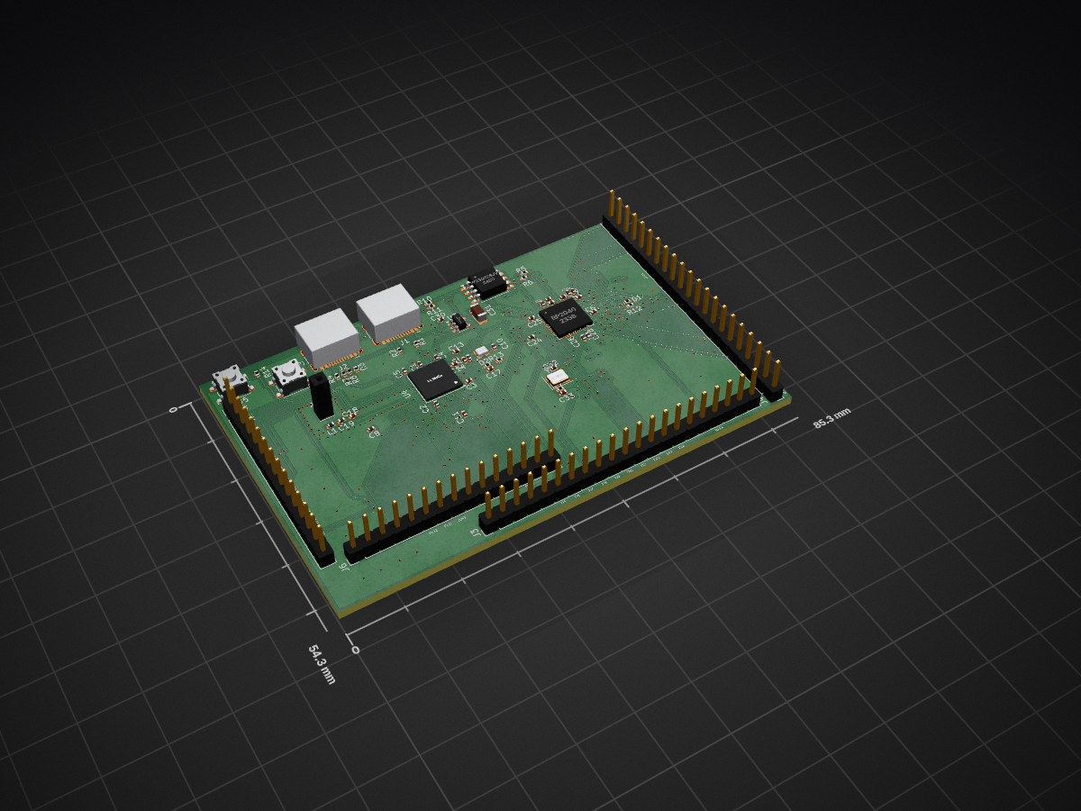
Bluetooth DevBoard is an open-source printed circuit board by GodOfStrategy, from the GodOfStrategy/Bluetooth-Devborad repository on GitHub, published under the MIT licence. It is a 4-layer board of 85.3 × 54.2 mm with 63 parts on 116 nets, routed with 1,697 tracks and 327 vias.
It is built around the RP2040, W25Q128JVSIQ and TLV75533PDBV, with the FA-128 among its other parts. Its parts include 31 capacitors, 14 resistors, 6 connectors, 4 ICs and 2 diodes. It belongs with the microcontroller boards and radio and wireless boards and the RP2040 boards of this library.


This is a cutom bluetooth devboard made by me for IoT and short range communication and automation.
This board uses a nRF 52840 QIAA-F-R7 along with a RP2040 for processing, wired together with SPI.
It also uses 2 crystals 12MHz and 32 MHz for thr Rp 2040 and the nRF 52840 respectively.
A TLV75533PDBV (LDO) as my Voltage regulator.
2 USB-C receptacles for programming both chips with firmware.
SMD resistors.
SMD capacitors.
Here is my schematic:
Here is my PCB:
Here is the 3D Imge of my PCB:
Here is my BoM of PCB components: BLE_DEV_001_bom.csv
Please find all production and firmware files in my repo.
| Qty | Value | Footprint | References |
|---|---|---|---|
| 8 | 0.1uF | Capacitor_SMD:C_0402_1005Metric | C7, C20, C21, C22, C23, C24, C25, C27 |
| 5 | 100 nF | Capacitor_SMD:C_0402_1005Metric | C1, C2, C3, C4, C5 |
| 4 | 1uF | Capacitor_SMD:C_0402_1005Metric | C11, C26, C28, C30 |
| 4 | 27 | Resistor_SMD:R_0402_1005Metric | R5, R6, R7, R8 |
| 4 | 5.1K | Resistor_SMD:R_0402_1005Metric | R1, R2, R3, R4 |
| 2 | 10K | Resistor_SMD:R_0402_1005Metric | R10, R14 |
| 2 | 12pF | Capacitor_SMD:C_0402_1005Metric | C9, C10 |
| 2 | 1K | Resistor_SMD:R_0402_1005Metric | R9, R11 |
| 2 | 330 | Resistor_SMD:R_0402_1005Metric | R12, R13 |
| 2 | 33pF | Capacitor_SMD:C_0402_1005Metric | C32, C33 |
| 2 | 4.7 uF | Capacitor_SMD:C_0402_1005Metric | C13, C14 |
| 2 | Conn_01x15_Pin | Connector_PinHeader_2.54mm:PinHeader_1x15_P2.54mm_Vertical | J5, J6 |
| 2 | LED | Diode_SMD:D_0402_1005Metric | D1, D2 |
| 2 | SW_Push | Button_Switch_SMD:SW_SPST_PTS647_Sx38 | RESET(nRF), SW1 |
| 2 | USB_C_Receptacle_USB2.0_16P | Connector_USB:USB_C_Receptacle_HCTL_HC-TYPE-C-16P-01A | J1, J2 |
| 1 | 0.1uF (C27-C28) | Capacitor_SMD:C_0402_1005Metric | C29 |
| 1 | 0.1uF (C6-25) | Capacitor_SMD:C_0402_1005Metric | C6 |
| 1 | 0.5 pF | Capacitor_SMD:C_0402_1005Metric | C19 |
| 1 | 0.8 pF | Capacitor_SMD:C_0402_1005Metric | C18 |
| 1 | 100nF | Capacitor_SMD:C_0402_1005Metric | C17 |
| 1 | 100pF | Capacitor_SMD:C_0402_1005Metric | C8 |
| 1 | 12 MHz | Crystal:Crystal_SMD_3225-4Pin_3.2x2.5mm | Y2 |
| 1 | 200uF | Capacitor_SMD:C_1206_3216Metric | C31 |
| 1 | 4.7nH | Inductor_SMD:L_0402_1005Metric | L1 |
| 1 | 4.7uF | Capacitor_SMD:C_0402_1005Metric | C12 |
| 1 | Ant | Connector_PinSocket_2.54mm:PinSocket_1x01_P2.54mm_Vertical | Ae1 |
| 1 | Conn_01x21_Pin (RP) | Connector_PinHeader_2.54mm:PinHeader_1x21_P2.54mm_Vertical | J4 |
| 1 | Conn_01x21_Pin(RP) | Connector_PinHeader_2.54mm:PinHeader_1x21_P2.54mm_Vertical | J3 |
| 1 | FA-128 | nRF5280-QFAA-R7:FA128 | Y1 |
| 1 | RP2040 | Package_DFN_QFN:QFN-56-1EP_7x7mm_P0.4mm_EP3.2x3.2mm | U2 |
| 1 | TLV75533PDBV | Package_TO_SOT_SMD:SOT-23-5 | U3 |
| 1 | W25Q128JVS | Package_SO:SOIC-8_5.3x5.3mm_P1.27mm | U1 |
| 1 | ~ | nRF5280-QFAA-R7:QIAA-F-R7 | U4 |
It measures 85.3 × 54.2 mm and has 4 copper layers, 1.6 mm thick.
63 parts, built around the RP2040, W25Q128JVSIQ, TLV75533PDBV and FA-128. The full list of its parts is on this page, with links to each part's symbol and footprint where PCBKit's library has them.
From the GodOfStrategy/Bluetooth-Devborad repository on GitHub, at the commit this page was made from: the board is Project Files/Bluetooth_DevBoard.kicad_pcb and its schematic Project Files/Bluetooth_DevBoard.kicad_sch. PCBKit opens the board in the browser, with nothing to install.
Its repository publishes it under the MIT licence: you may reuse it on that licence's terms (keep the author's notice, and for a copyleft licence share your changes alike).


minye065/imu-dev-board
A devboard that lets you test imu programs via the onboard imu and being able to test data to it

VarunAPatil/MedSafe
The goal: a compact, wrist-worn device that simultaneously tracks heart rate & SpO₂, motion & orientation, altitude & atmospheric pressure, and GNSS location — all in one tightly integrated system.


pustowhite/rp2040-logic-analyzer
An 8-channel RP2040 logic analyzer PCB designed in KiCad, with USB-C and selectable 1.8 V / 3.3 V input logic modes.