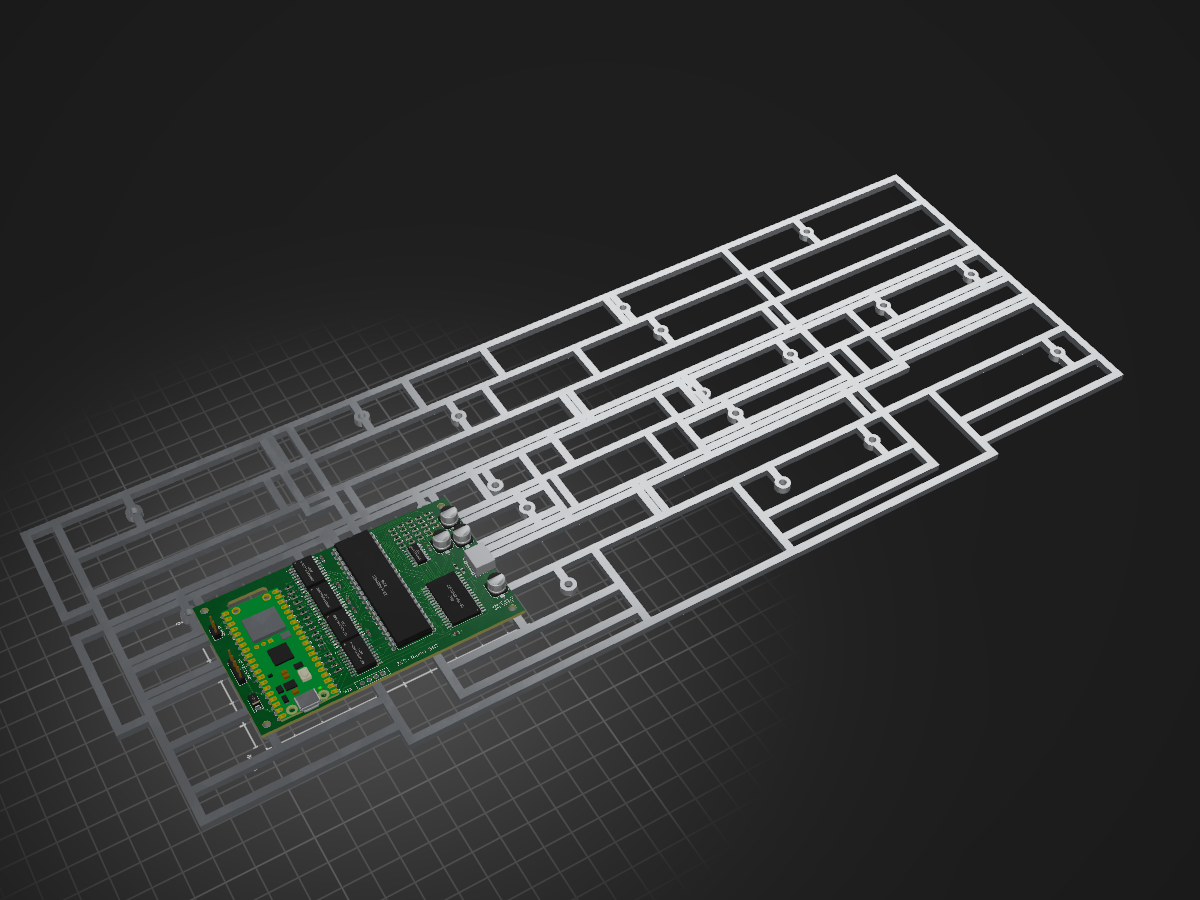
This is a separate KiCad project for a 98.3 × 60 mm, four-layer board. JLCPCB assembles every top-side SMT part, including the Raspberry Pi Pico 2 W module, and only four parts are hand-soldered:
Z80 romless sbc smt is an open-source printed circuit board by gloveboxes, from the gloveboxes/Z80ROMlessSBC repository on GitHub, published under the MIT licence. It is a 4-layer board of 98.3 × 60 mm with 70 parts on 73 nets, routed with 1,395 tracks and 251 vias.
It is built around the SN74LVC244ADWRE4, IS62C1024AL-35QLI and SS14. Its parts include 42 resistors, 11 capacitors, 7 ICs, 3 connectors and 1 diode. It belongs with the computers and single-board computers and retro computing and games boards and the RP2040 boards of this library.
This is a separate KiCad project for a 98.3 × 60 mm, four-layer board. JLCPCB
assembles every top-side SMT part, including the Raspberry Pi Pico 2 W module,
and only four parts are hand-soldered:
Ref
Part
Assembly
U1
Z84C0020PEC, DIP-40
Hand-soldered
A2
0.91 in SSD1315 OLED on a 1×4 2.54 mm female header, 5.0 mm body
Hand-soldered
J2
Pico GPIO expansion header, 1×4
Hand-soldered
J3
Auxiliary external 5 V header, 1×2
Hand-soldered
All other parts are JLCPCB-assembled from the LCSC numbers in the schematic:
SOIC logic and SOP-32 SRAM.
0603 resistors and capacitors.
SS14 diode.
SMT electrolytic capacitors.
Power-only USB-C receptacle with 5.1 kΩ CC pull-downs.
Raspberry Pi Pico 2 W (C42394205), reflowed on its castellated pads with
KiCad's RaspberryPi_Pico_W_SMD footprint.
The bulk capacitors are C8-C10 = 22 µF, 35 V (LCSC C150379) and C11 = 100 µF,
16 V (LCSC C346929). Both parts use the same 6.3 × 5.4 mm case, so they look
the same size in JLCPCB's placement preview; check the BOM part numbers and
values rather than judging capacitance from the rendered body size.
Sources
scripts/build-kicad-smt-schematic.py generates the schematic, symbols and
reports/net_manifest.json. Each component declares its assembly method,
jlc or hand. JLC parts must carry an LCSC number.
scripts/build-kicad-smt-pcb.py generates placement, rules, keepouts,
labels and 3D models. reports/z80_romless_sbc_smt.ses holds the accepted
Freerouting result.
scripts/export-jlc-assembly.py writes the JLCPCB BOM and CPL from the
manifest and the routed board.
Build and validate
Save and close the project in KiCad, then run from the repository root:
sh
PYTHON=.venv-kicad/bin/python npm run kicad:smt
The pipeline publishes exports/, fabrication/ and reports/ only after all
of these pass:
ERC and netlist/manifest parity.
PCB/DSN reproduction and zone-refilled DRC.
Route-length budgets.
The Gerber silk-to-mask audit (≥ 0.18 mm, target 0.20 mm).
Every track ≥ 0.155 mm from any solder-mask opening it does not connect
to. JLCDFM rates more than 0.15 mm as good.
The JLC BOM/CPL consistency check.
It does not modify hardware/kicad/.
JLCDFM design rules
Solder-mask openings are 0.05 mm per side larger than the copper. J1's
0.5 mm-pitch pads use 0.04 mm. JLCDFM flags 1:1 (zero-expansion) openings.
J1's signal pads are trimmed 0.05 mm narrower than the stock footprint.
This widens their copper gaps to 0.25 mm and leaves mask bridges of
0.17 mm. JLCDFM rates bridges of 0.15 mm or more as good; the generator
enforces 0.16 mm or a merged opening.
After the routing session is imported, the generator straightens
Freerouting's 45° pad exits. A run then cannot skim its own pad's mask
opening.
JLCDFM measures vias against rectangular pads as if the corners were
square. A via sitting diagonally off a rounded SOIC corner therefore
reports about 0.05 mm closer than it is. After import, the generator
nudges each such via (and its track ends) until it is ≥ 0.16 mm from
every square-cornered mask opening.
The Pico footprint keeps the library's landing pads for the module's
underside test points (TP1–TP6), SWD pads and USB shell legs. They are
unconnected, and routed copper clears them. The library's
"suggested RF board edge" keepouts are replaced by the enclosed antenna
window and bridge keepout; the antenna keepout itself is retained.
J1's stacked USB-C pad pairs (A1/B12, A4/B9, A9/B4, A12/B1) keep both
copper pads but emit one mask and paste opening each.
SMT pads sit at least 3.07 mm from other parts' through-hole pads.
JLCDFM rates more than 3.05 mm as good. J2 and J3 sit 2.85 mm from the
left edge so their pads clear the Pico castellations by 3.12 mm. J1's own shell legs are part of
the same footprint, and JLCDFM does not report them.
J1's plated shell slots are widened to 0.85 mm (1.9 mm and 1.75 mm long)
with a 0.2 mm annular ring. Each slot is moved 0.125 mm outward so its
inner edge stays at the stock position. JLCDFM rates slots wider than
0.81 mm as good; the generator enforces 0.82 mm and at least 2:1.
Dry-fit the purchased C393939 before ordering.
The outline, including the enclosed Pico antenna window.
The job file.
Separate plated and non-plated millimetre Excellon drill files.
The full BOM (z80_romless_sbc_smt-bom.csv, including hand-soldered parts),
the KiCad position file, IPC-D-356 netlist, drill maps and report sit next to
the ZIP; they are not uploaded.
JLCPCB order settings
PCB:
FR-4, 4 layers, 1.6 mm, 98.3 × 60 mm.
Layer order: front, GND, +5 V, back.
1 oz outer and 0.5 oz inner copper.
LeadFree HASL, green mask and white silk.
The antenna window is an enclosed through-cutout, not a slot to the edge.
A 4 mm FR-4 bridge keeps the top edge continuous.
The smallest drill is the 0.4 mm via; the USB-C shell uses four 0.85 mm
plated slots.
PCBA:
Top side only.
Economic PCBA. The 60 mm board height is below Standard PCBA's
70 × 70 mm single-board minimum. Standard PCBA would require a panel with
edge rails and fiducials.
Upload the JLC BOM and CPL listed above. The four hand-soldered parts are
intentionally absent from both files.
The Pico 2 W (C42394205) is an Extended part that JLCPCB requires X-ray
inspection for. Pre-order it into your JLCPCB parts library if it is not
in stock.
Before ordering
Check every part's rotation in JLCPCB's placement preview. The CPL
applies the community kicad-jlcpcb-tools correction table:
SOIC/SOP: +270°.
CP_Elec: 0°. The community +180° rule reversed C150379/C346929 in
JLC's preview.
HRO-pattern USB-C: 0°, placed at its copper pad centre (1.5 mm inboard
of the KiCad origin). The community +180° rule turned C393939's mouth
inward in JLC's preview.
Pico 2 W module: +270°. There is no community rule for C42394205;
JLC's preview showed its model at 0° with the USB end to the left.
SMA and 0603: 0°.
Specifically confirm:
Pin 1 on U2, U3, U4, U7, U9 and U10.
The + lead on C8–C11.
The cathode band on D1, which faces Pico VSYS.
The USB-C mouth on J1, which faces the board edge.
The Pico 2 W's micro-USB connector, which faces the bottom edge, and
its antenna over the enclosed window.
Confirm stock for U2 (IS62C1024AL-35QLI, C397875, Extended and low stock)
and the other Extended parts at order time.
Confirm JLCPCB quotes J1's shell legs as part of the SMT assembly.
Dry-fit the purchased OLED header. It must accept the module's square pins
and fit the 1.0 mm holes.
Physical bring-up starts at 1 MHz. Fabrication acceptance is not 20 MHz
timing qualification.
This is a separate KiCad project for a 98.3 × 60 mm, four-layer board. JLCPCB assembles every top-side SMT part, including the Raspberry Pi Pico 2 W module, and only four parts are hand-soldered:
The Smart Plant is a board that can be plugged directly on the soil, close to the plant, that allows the measurement of the environment (soil moisture, environment temperature & illuminance), and presents the…
Drone Show Software is software designed for drone shows, allowing flight path planning as well as control of dozens of drones simultaneously in a synchronized manner.
PCB files for ZeroPhone - for gerbers and schematics, go to "Releases" tab!
118 parts148GPL-3.0
Questions
How big is the Z80 romless sbc smt PCB?
It measures 98.3 × 60 mm and has 4 copper layers, 1.6 mm thick.
What parts does the Z80 romless sbc smt use?
70 parts, built around the SN74LVC244ADWRE4, IS62C1024AL-35QLI and SS14. The full list of its parts is on this page, with links to each part's symbol and footprint where PCBKit's library has them.
Where can I download the Z80 romless sbc smt KiCad files?
From the gloveboxes/Z80ROMlessSBC repository on GitHub, at the commit this page was made from: the board is hardware/kicad-smt/z80_romless_sbc_smt.kicad_pcb and its schematic hardware/kicad-smt/z80_romless_sbc_smt.kicad_sch. PCBKit opens the board in the browser, with nothing to install.
Can I use the Z80 romless sbc smt design in my own project?
Its repository publishes it under the MIT licence: you may reuse it on that licence's terms (keep the author's notice, and for a copyleft licence share your changes alike).