
2 layers231.1 × 106.7 mm

 gfoot/homebrewkeyboard10
Schematics, board layouts, and code for adding a homebrew keyboard to your electronics projects
Keyboard vero2 is an open-source printed circuit board by gfoot, from the gfoot/homebrewkeyboard repository on GitHub, published under the Unlicense licence. It is a 4-layer board of 162.6 × 99.1 mm with 85 parts on 39 nets, routed with 569 tracks and 187 vias.
It is built around the 74LS374PC. Its parts include 66 switches, 8 resistors, 8 diodes, 2 ICs and 1 connector. It belongs with the keyboards and input boards of this library.
Schematics, board layouts, and code for adding a homebrew keyboard to your electronics projects
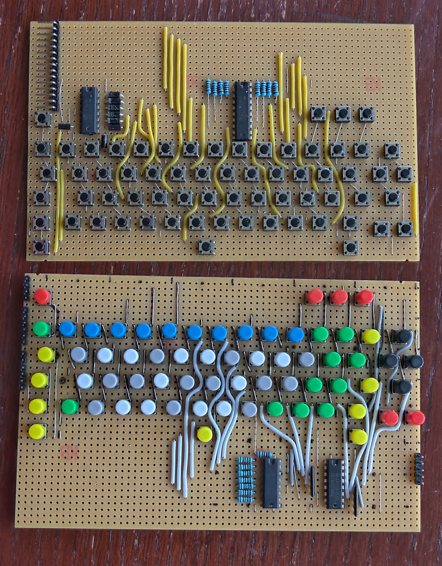
This one uses a parallel interface, ideal for connecting directly to the address and data bus of something like a 6502.
I also have one with a serial interface, more tailored for Arduino - let me know if you're interested and I'll publish it as a separate project.
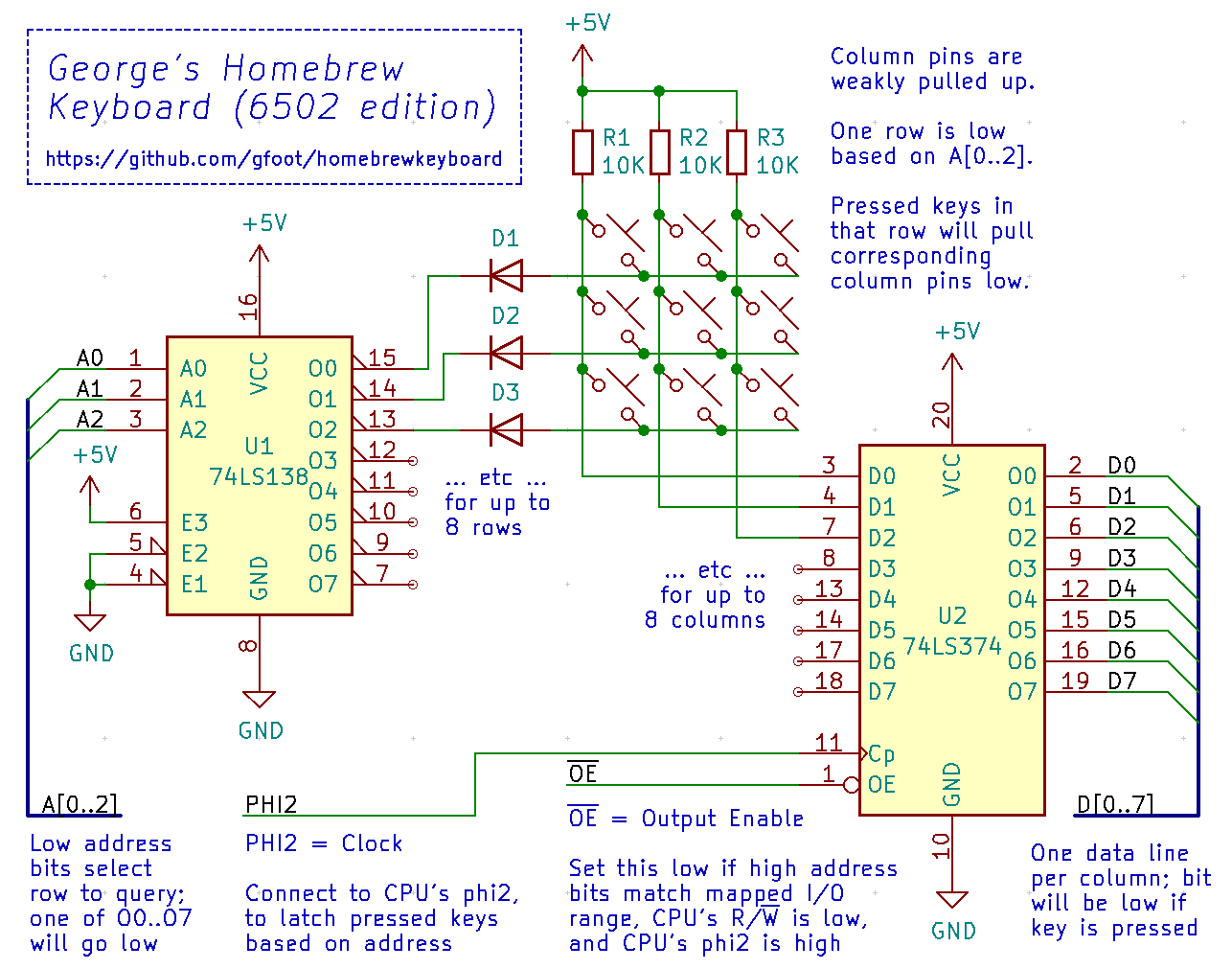
Connect:
~OE needs to be kept high unless all of the following are true:
For the last one, my own 6502 computer simply uses an LS138 fed by the top three address lines, and one of the LS138's outputs drives this logic - the same way I generate chip-select signals for other memory-mapped parts of the computer.
Then the CPU can simply read from the mapped addresses. The lowest address - for example, $a000 - corresponds to one "row" of keys; each bit is 1 if the corresponding key is not pressed, and 0 if it is pressed. The next address, $a001, corresponds to the next "row", up to the final row at $a007. The word "row" refers to the schematic, not the physical layout.
As an example, the shift keys correspond to bit 1 of $a000; the ctrl keys correspond to bit 3. I think bit 0 is Esc, and bit 2 is the space bar. $a001's bit 0 corresponds to the tilde/backtick key; bit 1 is probably tab or Q; bit 2 is A; and so on. The exact layout was tweaked to make it easier to build on veroboard, while also ensuring that rollover works well with modifier keys in particular; as usual for this sort of thing, you need to do a lot more translation in software.
See the kbd module which contains a full table of characters by row/column.
See sample code and kbd module.
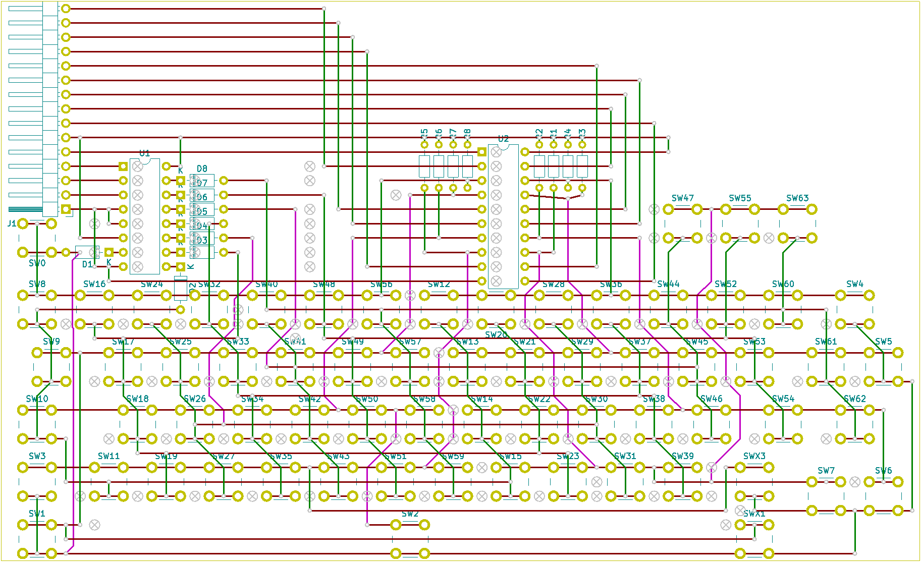
The board layout shows the physical layout of the components. The veroboard tracks run horizontally, and - where they are used - they are shown in dark red. Green traces indicate fairly short links, mostly made with bare wire. Pink traces indicate longer insulated wire links. The (X) marks show where you need to break the existing veroboard tracks.
Some connections occur underneath switches, or pass entirely under a switch. This doesn't always work well in practice, and I ended up routing some wires differently to this diagram. It depends on the thickness of the wire and the physical shape of your switches.
| Qty | Value | Footprint | References |
|---|---|---|---|
| 66 | SW_Push_45deg | keyboard_vero2:SW_PUSH_6mm | SW0, SW1, SW2, SW10, SW11, SW12, SW13, SW14, SW15, SW16, SW17, SW18, SW19, SW20, SW21, SW22 +50 |
| 8 | 10K | Resistor_THT:R_Axial_DIN0204_L3.6mm_D1.6mm_P7.62mm_Horizontal | R1, R2, R3, R4, R5, R6, R7, R8 |
| 8 | 1K | Diode_THT:D_DO-35_SOD27_P7.62mm_Horizontal | D1, D2, D3, D4, D5, D6, D7, D8 |
| 1 | 74LS138 | Package_DIP:DIP-16_W7.62mm | U1 |
| 1 | 74LS374 | Package_DIP:DIP-20_W7.62mm | U2 |
| 1 | Conn_01x15_Male | Connector_PinHeader_2.54mm:PinHeader_1x15_P2.54mm_Horizontal | J1 |

tjboldt/ProDOS-ROM-Drive
A bootable 1 MB solid state disk for Apple ][ computers

hkzlab/CGA_Redux
The Color Graphics Adapter Redux board is a more or less faithful clone of the original IBM CGA, based on the original schematics


alvaroalea/plusD-clone
Schematic of a clone of the Disk Interface +D for the ZX Spectrum

fortinsylvain/MyCpu
Home brew CPU Hardware with 1-bit ALU implementation using 74LSxx, a micro-code and assembler coded in C#.

raymondh2/CompaqPortableIII
Current PCB Memory Expansion board layout is untested. The backplane for the expansion cards is tested and working.
It measures 162.6 × 99.1 mm and has 4 copper layers, 1.6 mm thick.
85 parts, built around the 74LS374PC. The full list of its parts is on this page, with links to each part's symbol and footprint where PCBKit's library has them.
From the gfoot/homebrewkeyboard repository on GitHub, at the commit this page was made from: the board is keyboard_vero2/keyboard_vero2.kicad_pcb. PCBKit opens the board in the browser, with nothing to install.
Its repository publishes it under the Unlicense licence: you may reuse it on that licence's terms (keep the author's notice, and for a copyleft licence share your changes alike).