
4 layers16.9 × 119.4 mm

 Genexiz/USB2.0CtoA
Practicing my schematic and PCB design skills
USBCtoA2 0 is an open-source printed circuit board by Genexiz, from the Genexiz/USB2.0CtoA repository on GitHub. It is a 2-layer board of 30 × 16 mm with 9 parts on 11 nets, routed with 101 tracks and 2 vias.
It is built around the USBLC6-2SC6. Its parts include 3 capacitors, 2 resistors, 2 connectors, 1 IC and 1 fuse.
Work in Progress USBC to A Adapter (USB2.0) with 2-layers PCB
This is my hobby project for practicing circuit design and PCB design skills
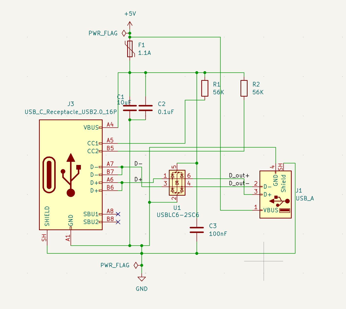
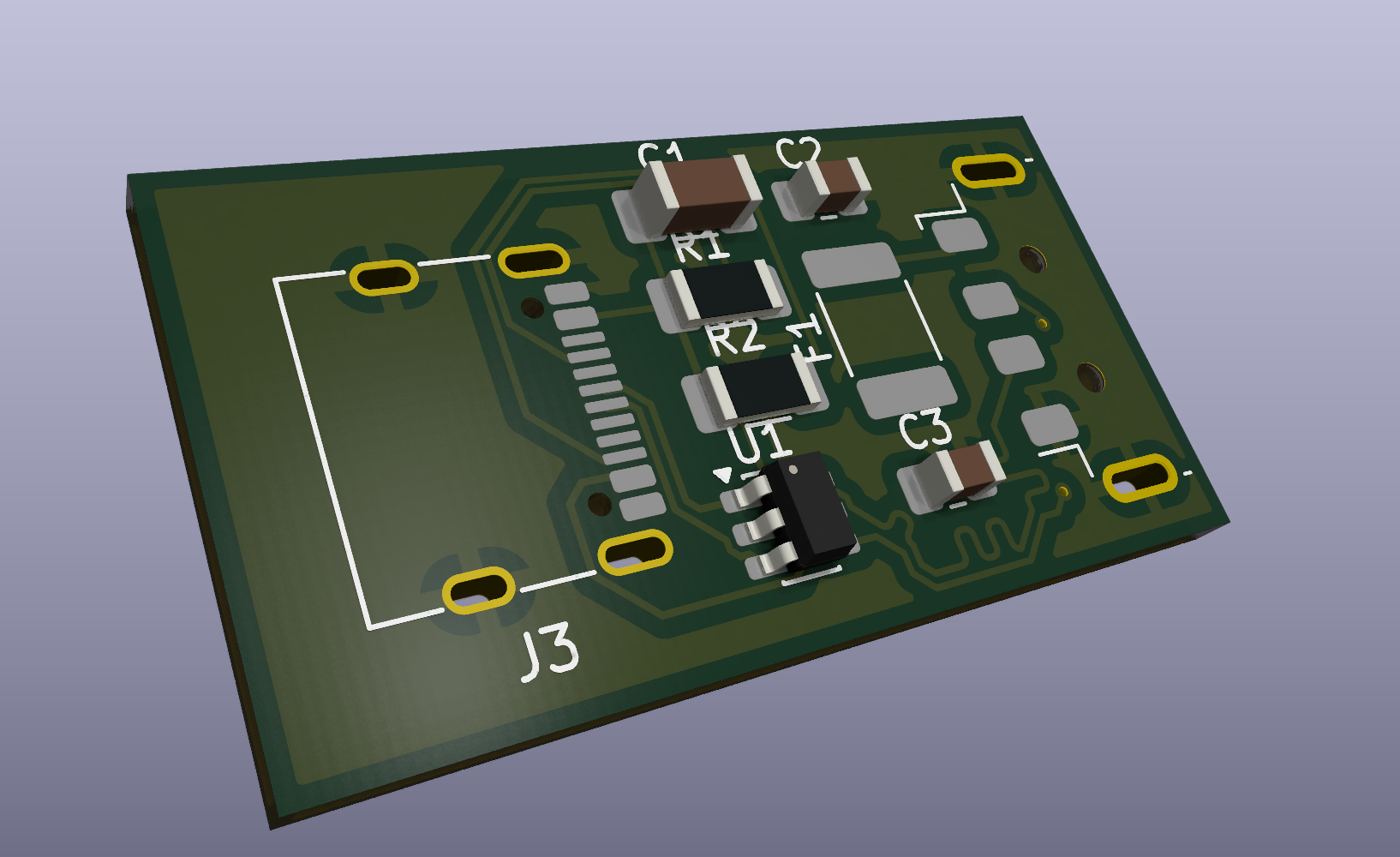
AI used in this project -> Gemini 3.7 flash (For suggest method how to design a schematic)
| Qty | Value | Footprint | References |
|---|---|---|---|
| 2 | 56K | Resistor_SMD:R_1206_3216Metric_Pad1.30x1.75mm_HandSolder | R1, R2 |
| 1 | 0.1uF | Capacitor_SMD:C_0805_2012Metric_Pad1.18x1.45mm_HandSolder | C2 |
| 1 | 1.1A | Fuse:Fuse_1812_4532Metric_Pad1.30x3.40mm_HandSolder | F1 |
| 1 | 100nF | Capacitor_SMD:C_0805_2012Metric_Pad1.18x1.45mm_HandSolder | C3 |
| 1 | 10uF | Capacitor_SMD:C_1206_3216Metric_Pad1.33x1.80mm_HandSolder | C1 |
| 1 | USBLC6-2SC6 | Package_TO_SOT_SMD:SOT-23-6 | U1 |
| 1 | USB_A | Connector_USB:USB_A_Molex_48037-2200_Horizontal | J1 |
| 1 | USB_C_Receptacle_USB2.0_16P | Connector_USB:USB_C_Receptacle_G-Switch_GT-USB-7010ASV | J3 |


TalismanDesign/PocketMage_PDA
An E-Ink PDA device using the ESP32 S3.


shorepine/tulipcc
The Tulip Creative Computer and AMYboard - portable Python synthesizers


LeoDJ/FW-EC-DongleHiderPlus
Framework Expansion Card that includes a USB hub to hide a bare dongle inside and still have a USB-A port externally
It measures 30 × 16 mm and has 2 copper layers, 1.6 mm thick.
9 parts, built around the USBLC6-2SC6. The full list of its parts is on this page, with links to each part's symbol and footprint where PCBKit's library has them.
From the Genexiz/USB2.0CtoA repository on GitHub, at the commit this page was made from: the board is USBCtoA2_0.kicad_pcb and its schematic USBCtoA2_0.kicad_sch. PCBKit opens the board in the browser, with nothing to install.
Its repository states no licence, so its author keeps all rights: ask Genexiz before reusing the design.