

2 layers305.2 × 76.2 mm

 geek-rabb1t/futaba27
Futaba is a keyboard with trackpad.
Futaba pcb is an open-source printed circuit board by geek-rabb1t, from the geek-rabb1t/futaba repository on GitHub, published under the MIT licence. It is a 2-layer board of 317.2 × 109.9 mm with 106 parts on 75 nets, routed with 1,866 tracks and 46 vias.
It is built around the RP2040-ZERO and 1N4148W. Its parts include 50 diodes, 49 switches, 2 resistors, 1 IC and 1 connector. It belongs with the keyboards and input boards and the RP2040 boards of this library.
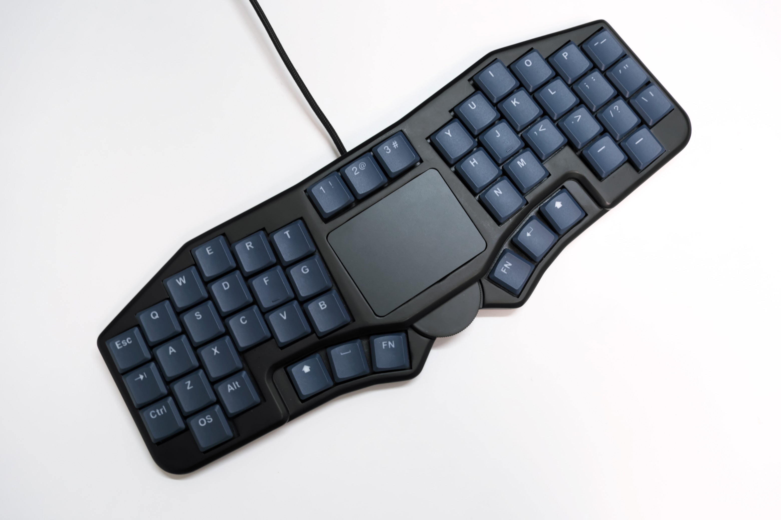
Futaba is a keyboard with trackpad.
This repository contains hardware design data only.
QMK firmware or Vial firmware can be obtained from the following URL
Please read here.
Futabaはトラックパッド付きキーボードです。
このリポジトリにはハードウェアの設計データのみ格納しています。
以下のURLにQMK Firmwareもしくは、 Vialのファームウェアがあります。
こちらをご覧ください。
| Qty | Value | Footprint | References |
|---|---|---|---|
| 50 | 1N4148W | Diode_SMD:D_SOD-123 | D1, D2, D10, D11, D12, D13, D14, D15, D16, D17, D18, D19, D20, D21, D22, D23 +34 |
| 23 | SW_Push | keyboard:Choc_Socket-flex-drill | SW10, SW11, SW12, SW13, SW14, SW15, SW16, SW17, SW18, SW31, SW32, SW33, SW34, SW35, SW36, SW37 +7 |
| 15 | SW_Push | keyboard:Choc_Socket-flex-drill_top | SW1, SW2, SW3, SW4, SW5, SW6, SW25, SW26, SW27, SW28, SW29, SW30, SW49, SW50, SW51 |
| 6 | SW_Push | keyboard:Choc_Socket-flex-drill_mid | SW22, SW23, SW24, SW46, SW47, SW48 |
| 5 | SW_Push | keyboard:Choc_Socket-flex-drill_bottom | SW20, SW21, SW42, SW44, SW45 |
| 2 | 1kΩ | Resistor_SMD:R_0603_1608Metric | R1, R2 |
| 1 | Conn_01x06 | keyboard:Jushuo_AFC07-S06FCA-00_1x6-1MP_P0.50_Horizontal-JLC | J1 |
| 1 | MountingHole_3.2mm_M3_ISO14580_Pad_TopBottom | MountingHole:MountingHole_3.2mm_M3_ISO14580_Pad_TopBottom | Clicker |
| 1 | RP2040-Zero | keyboard:RP2040-Zero | U1 |
| 1 | RotaryEncoder | Rotary_Encoder:RotaryEncoder_Alps_EC12E_Vertical_H20mm | EC12 |
| 1 | SW_SPDT_312 | keyboard:MicroSwitch | MSW1 |

sebastian-stumpf/narfkb
rp2040 powered split keyboard with rotary encoders and 6mm tactile buttons


sago35/keyboards
This repository was created to manage the circuitry and firmware for the keyboards I designed. The firmware is created using sago35/tinygo-keyboard.


It measures 317.2 × 109.9 mm and has 2 copper layers, 1.6 mm thick.
106 parts, built around the RP2040-ZERO and 1N4148W. The full list of its parts is on this page, with links to each part's symbol and footprint where PCBKit's library has them.
From the geek-rabb1t/futaba repository on GitHub, at the commit this page was made from: the board is pcb/futaba-pcb.kicad_pcb and its schematic pcb/futaba-pcb.kicad_sch. PCBKit opens the board in the browser, with nothing to install.
Its repository publishes it under the MIT licence: you may reuse it on that licence's terms (keep the author's notice, and for a copyleft licence share your changes alike).