
2 layers107 × 80 mm

 g200kg/multiribbon2
PCB Keys is an open-source printed circuit board by g200kg, from the g200kg/multiribbon repository on GitHub, published under the MIT licence. It is a 2-layer board of 310 × 60 mm with 135 parts on 80 nets, routed with 552 tracks and 18 vias.
It is built around the MMA8452QT. Its parts include 65 resistors, 60 switches, 2 capacitors, 2 connectors and 1 IC.
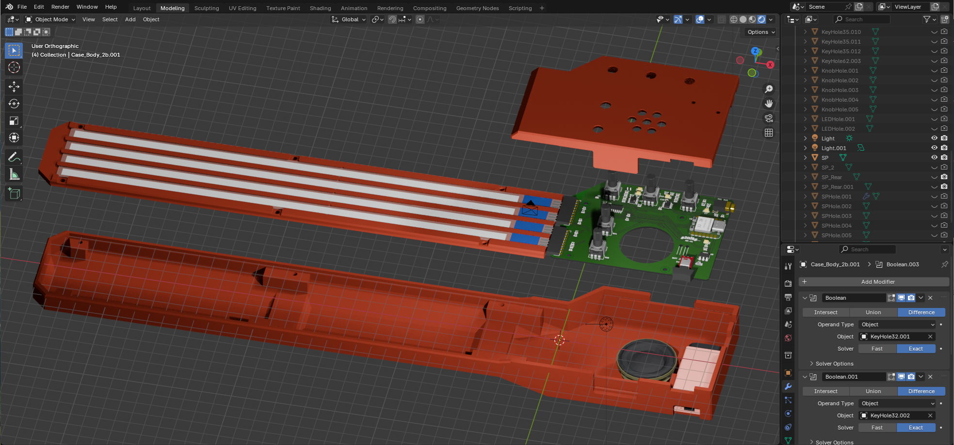
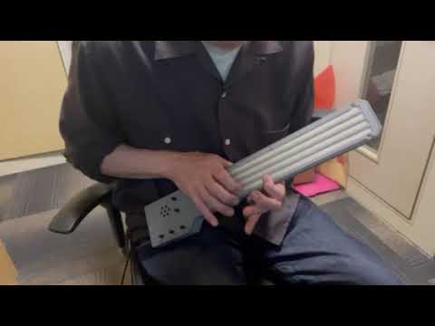
現在開発中の謎楽器です。
複数のリボンコントローラーを並列に並べたフレットレスなギターのような演奏を想定しています。
MCU として XIAO RA4M1 を使用
| Qty | Value | Footprint | References |
|---|---|---|---|
| 60 | SW_Push | MyLib:Sw_Push_12x12_SMD | SW1, SW2, SW10, SW11, SW12, SW13, SW14, SW15, SW16, SW17, SW18, SW19, SW20, SW21, SW22, SW23 +44 |
| 56 | 1K | Resistor_SMD:R_0603_1608Metric | R1, R2, R10, R11, R12, R13, R14, R15, R16, R17, R18, R19, R20, R21, R22, R23 +40 |
| 5 | 10K | Resistor_SMD:R_0603_1608Metric | R57, R58, R59, R60, R65 |
| 4 | 220R | Resistor_SMD:R_0603_1608Metric | R61, R62, R63, R64 |
| 4 | Hole | MountingHole:MountingHole_3.2mm_M3_DIN965_Pad | H1, H2, H3, H4 |
| 2 | 0.1uF | Capacitor_SMD:C_0603_1608Metric | C1, C2 |
| 2 | Conn_01x10 | Connector_PinHeader_2.54mm:PinHeader_1x10_P2.54mm_Horizontal | J1, J2 |
| 1 | LOGO | MyLib:g200kgLogo | LG1 |
| 1 | MMA8452Q | MyLib:QFN16_3x3mm_MMA8452Q | U1 |


bnahill/wireless_logger
A compact wireless inertial logging and processing hardware platform

AEFeinstein/Super-2020-Swadge-HW
The hardware for a hardware badge (Swadge) for Magfest 2020


jkravanja/heart_rate_monitor
Heart rate monitor designed in KiCad, using Nordic NRF51822 bluetooth module and TI AFE4400 heart rate module.

It measures 310 × 60 mm and has 2 copper layers, 1.6 mm thick.
135 parts, built around the MMA8452QT. The full list of its parts is on this page, with links to each part's symbol and footprint where PCBKit's library has them.
From the g200kg/multiribbon repository on GitHub, at the commit this page was made from: the board is PCB/PCB_Keys/PCB_Keys.kicad_pcb and its schematic PCB/PCB.kicad_sch. PCBKit opens the board in the browser, with nothing to install.
Its repository publishes it under the MIT licence: you may reuse it on that licence's terms (keep the author's notice, and for a copyleft licence share your changes alike).