
4 layers312 × 106.7 mm

 frubem/TK2000_FASTIDIO
Forked from https://codeberg.org/hkzlab/TK2000_FASTIDIO
TK2000 FASTIDIO is an open-source printed circuit board by frubem, from the frubem/TK2000_FASTIDIO repository on GitHub, published under the CC-BY-SA-4.0 licence. It is a 2-layer board of 124.3 × 82.4 mm with 29 parts on 112 nets, routed with 763 tracks and 148 vias.
It is built around the 74LS245SC and BAT46. Its parts include 6 capacitors, 6 connectors, 5 ICs and 2 diodes.
Any use of this project is under your own responsibility. You will be responsible of checking the correct construction and functionality of your board. By using this project You will agree that I cannot be held responsible if it will destroy any of your devices, damage your computer, burn down your house or whatever.

This project is kindly sponsored by PCBWay. PCBWay specializes in manufacturing high-quality PCBs and makes them affordable to hobbyist and professionals alike.
The range of services they offer include PCB prototyping, assembly, instant quotes for your order, a verification process by a team of experts and an easy to use, hassle-free order process.
I'm grateful to PCBWay for the help in evolving and testing this project. You can order the currently released revisions of the board from them, see the link below!
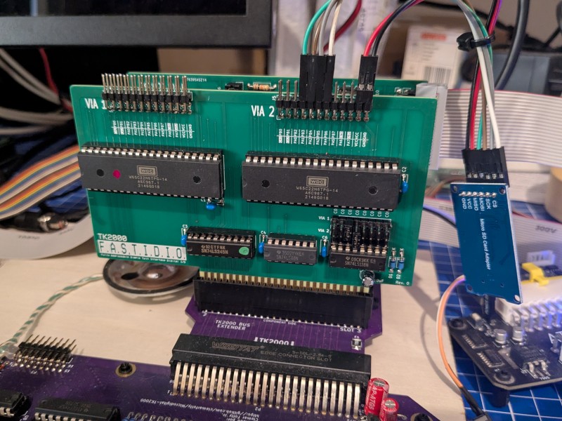
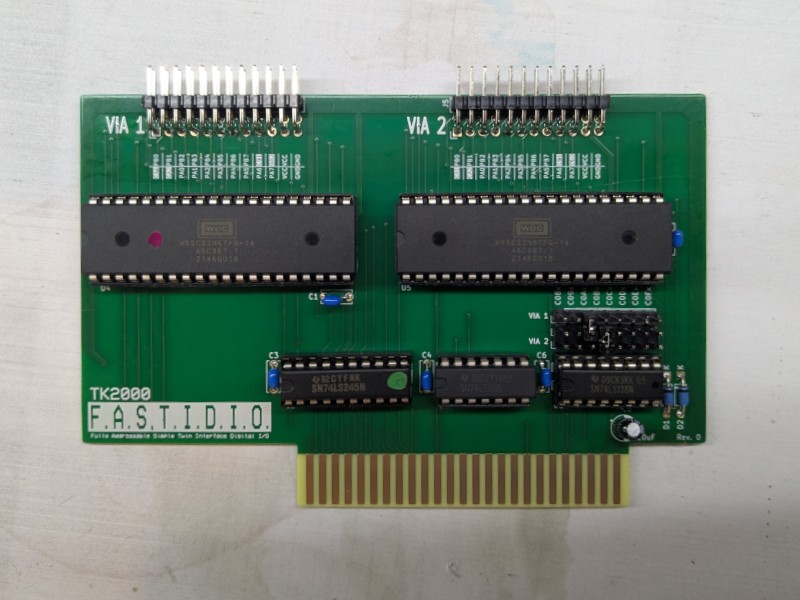
The F.A.S.T.I.D.I.O. (Fully Addressable Simple Twin Interface Digital I/O) is an expansion card for the TK2000 computer that provides two 6522 VIAs to the computer.
Using 6522, you gain timers, and 4 8-bit I/O ports that can be used, for example, to interface with gamepads, or SD cards. All the I/O ports are broken out to pin headers. Additionally, the address of each 6522 can be set independently (and either of the VIAs can be left out entirely).
This board is meant to be used in the TK2000 bus extender and is part of my project to build a set of cards for the TK2000 computer.
You can build yourself a TK2000 computer using files from this repo and following my build notes.
If you wish to support me in building new hardware and software for old machines, throw a few euros in my direction via Ko-Fi ☕!
The board was designed with KiCad EDA.
| Component | Qty | Type / Value | Notes |
|---|---|---|---|
| U1 | 1 | 74LS138 DIP-16 | HCT/ACT can also be used, but see note below |
| U2 | 1 | 74LS245 DIP-20 | OPTIONAL: HCT/ACT can also be used, but see note below |
| U3 | 1 | 74LS08 DIP-14 | OPTIONAL: HCT/ACT can also be used, but see note below |
| U4, U5 | 2 | 6522 DIP-40 | W65C22N and SY6522A tested |
| C5 | 1 | 10uF/16V+ 2.5mm electrolytic capacitor | |
| C1 - C4, C6 | 5 | 100nF/25V+ 5.0mm ceramic caps | |
| J1, J2, J3 | 3 | 1x8 2.54mm pin header, straight | |
| J4, J5 | 2 | 2x12 2.54mm pin header, right angle | |
| D1, D2 | 2 | BAT46 DO-35 | Any Schottky is probably going to work perfectly fine |
I noticed that access timing might be a bit finicky in regard to the Φ2 clock coming from the TK2000.
Experimenting, I found I the best reliability installing a 330pF capacitor (there is a provision for such capacitor on the BUS Extender) between Φ2 and GND and bypassing U2.
Once U2 is bypassed, U3 is also no longer needed and can be left off the board. Since rev.3 onward, you can bypass U2 by soldering the jumpers behind U2 (solder side). On previous revisions (0 to 2), you need to bridge the data lines yourself, like this:
My advice is to actually avoid installing U2 and U3 altogether and bypass them: use them only if an additional transceiver on the bus is later found necessary.
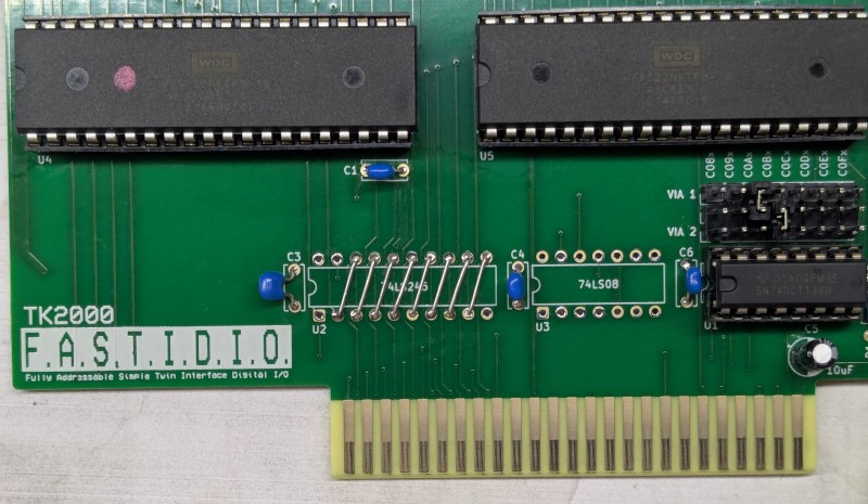
The address for the I/O ports can be changed by jumpering the VIA 1/VIA 2 headers to the middle row.
      C C C C C C C C
      0 0 0 0 0 0 0 0
      8 9 A B C D E F
	  x x x x x x x x
VIA 1 . . | . . . . .
      . . | | . . . .
VIA 2 . . . | . . . .
          ^ default for VIA 1
^ default for VIA 2You can order the board for this project at PCBWay and support me or download the gerbers and have them printed wherever you like!!!
| Qty | Value | Footprint | References |
|---|---|---|---|
| 8 | Jumper_2_Small_Open | Jumper:SolderJumper-2_P1.3mm_Open_RoundedPad1.0x1.5mm | JP3, JP4, JP5, JP6, JP7, JP8, JP9, JP10 |
| 5 | 100nF | Capacitor_THT:C_Disc_D6.0mm_W2.5mm_P5.00mm | C1, C2, C3, C4, C6 |
| 2 | 6522 | Package_DIP:DIP-40_W15.24mm | U4, U5 |
| 2 | BAT46 | Diode_THT:D_DO-35_SOD27_P7.62mm_Horizontal | D1, D2 |
| 2 | Diode Bypass | Jumper:SolderJumper-2_P1.3mm_Open_RoundedPad1.0x1.5mm | JP1, JP2 |
| 1 | 10uF | Capacitor_THT:CP_Radial_D5.0mm_P2.50mm | C5 |
| 1 | 74LS08 | Package_DIP:DIP-14_W7.62mm | U3 |
| 1 | 74LS138 | Package_DIP:DIP-16_W7.62mm | U1 |
| 1 | 74LS245 | Package_DIP:DIP-20_W7.62mm | U2 |
| 1 | Base Address | Connector_PinHeader_2.54mm:PinHeader_1x08_P2.54mm_Vertical | J1 |
| 1 | Expansion Edge | TK2000:Conector Edge | P1 |
| 1 | VIA1 I/O | Connector_PinHeader_2.54mm:PinHeader_2x12_P2.54mm_Horizontal | J4 |
| 1 | VIA2 I/O | Connector_PinHeader_2.54mm:PinHeader_2x12_P2.54mm_Horizontal | J5 |
| 1 | VIA_SEL_1 | Connector_PinHeader_2.54mm:PinHeader_1x08_P2.54mm_Vertical | J2 |
| 1 | VIA_SEL_2 | Connector_PinHeader_2.54mm:PinHeader_1x08_P2.54mm_Vertical | J3 |
It measures 124.3 × 82.4 mm and has 2 copper layers, 1.6 mm thick.
29 parts, built around the 74LS245SC and BAT46. The full list of its parts is on this page, with links to each part's symbol and footprint where PCBKit's library has them.
From the frubem/TK2000_FASTIDIO repository on GitHub, at the commit this page was made from: the board is TK2000_FASTIDIO.kicad_pcb and its schematic TK2000_FASTIDIO.kicad_sch. PCBKit opens the board in the browser, with nothing to install.
Its repository publishes it under the CC-BY-SA-4.0 licence: you may reuse it on that licence's terms (keep the author's notice, and for a copyleft licence share your changes alike).

cyberboy666/recurBOY
a rpi0 video-instrument – created in collaboration with Guergana Tzatchkova

cyberboy666/sync_ope
effect send + sync restoring circuit - adapted from a gael jaton design

robsonsmartins/usbflashprog
A memory device programmer (Flash/EPROM/E2PROM) board and software, connected to PC by USB port.

mariusgreuel/EMS-Bus-Gateway
EMS Bus Gateway for Buderus Boilers to run EMS-ESP32

cyberboy666/i_n_c_u_r
a r_e_c_u_r video sampler extension circuit - adding knobs, cv and serial midi control

CosmicPi/CosmicPiV1.7PCB
PCB for Version 1.7 of the Cosmic Pi Hardware. Incremental changes from V1.6. This design is licensed under the CERN OHL V1.2
