2 layers64 × 39 mm

 freeDSP/SigmaLink-USBi33
The freeDSP SigmaLink USBi PROGRAMMER is an all-in-one real-time programming interface.
SigmaLink USBi is an open-source printed circuit board by freeDSP, from the freeDSP/SigmaLink-USBi repository on GitHub, published under the CC-BY-SA-4.0 licence. It is a 2-layer board of 64 × 39 mm with 31 parts on 39 nets, routed with 307 tracks and 556 vias.
It is built around the 24LC512-I/P, 74LVC2G66DP and LM1117-3.3, with the MAX809S, TPS2051BD and B5819W among its other parts. Its parts include 10 capacitors, 6 ICs, 4 diodes, 3 connectors and 2 resistors. It belongs with the interfaces and adapters boards of this library.


The SigmaLink USBi is an all-in-one real-time programming interface.
MAIN COORDINATOR: Max Chan
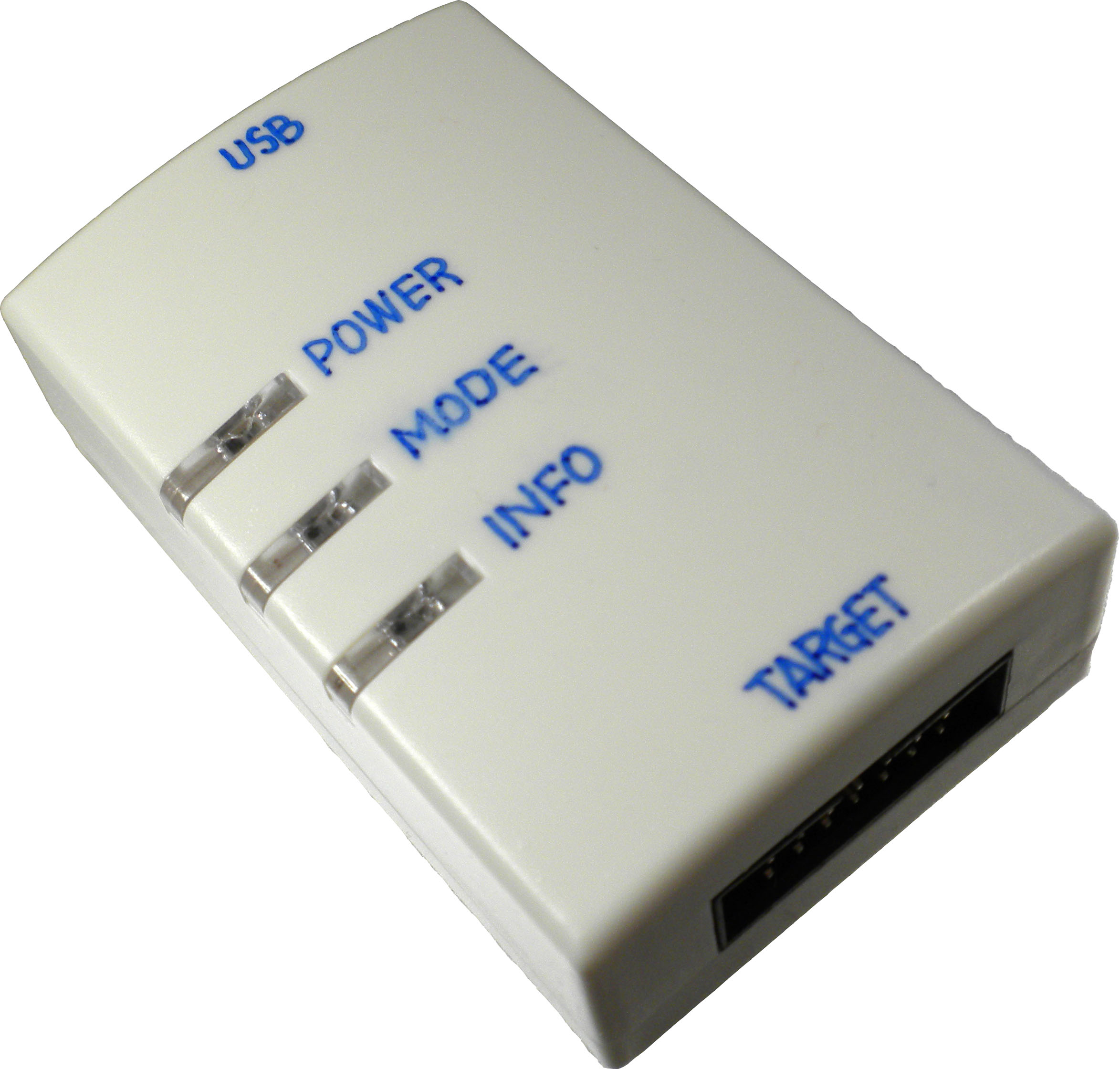
The SigmaLink USBi is a low-budget real-time programming device for the freeDSP and other DSP boards from Analog Devices. It is a new PCB design based on a CY7C68013 chip.
It has the same features as the Analog Devices USB interface (EVAL-ADUSB2EBZ), such as changing parameters while already using the freeDSP or easy changes of the schematic in SigmaStudio. You also can write your program to the EEPROM.
Please refer to the documentation for more information:
This work and all other materials under https://github.com/freeDSP are licensed under a Creative Commons Attribution Share-Alike 4.0 license. This allows for both personal and commercial derivative works, as long as they credit freeDSP and release their designs under the same license.
| Qty | Value | Footprint | References |
|---|---|---|---|
| 6 | 100n | Capacitor_SMD:C_0603_1608Metric_Pad1.05x0.95mm_HandSolder | C5, C6, C7, C9, C11, C13 |
| 2 | 22p | Capacitor_SMD:C_0603_1608Metric_Pad1.05x0.95mm_HandSolder | C3, C4 |
| 2 | 4.7k | Resistor_SMD:R_Array_Convex_4x0603 | RN2, RN4 |
| 1 | 100µ | Capacitor_SMD:CP_Elec_6.3x5.3 | C1 |
| 1 | 10k | Resistor_SMD:R_Array_Convex_4x0603 | RN3 |
| 1 | 220µ | Capacitor_SMD:CP_Elec_6.3x5.3 | C2 |
| 1 | 24LC512 | Package_SO:SOIC-8_3.9x4.9mm_P1.27mm | U2 |
| 1 | 24MHz | Crystal:Crystal_HC49-4H_Vertical | Y1 |
| 1 | 4.7k | Resistor_SMD:R_0603_1608Metric_Pad1.05x0.95mm_HandSolder | R7 |
| 1 | 49.9 | Resistor_SMD:R_0603_1608Metric_Pad1.05x0.95mm_HandSolder | R6 |
| 1 | 500mA | Fuse:Fuse_1812_4532Metric_Pad1.30x3.40mm_HandSolder | F1 |
| 1 | 510 | Resistor_SMD:R_Array_Convex_4x0603 | RN1 |
| 1 | 74LVC2G66 | Package_SO:VSSOP-8_3.0x3.0mm_P0.65mm | U5 |
| 1 | B5819W | Diode_SMD:D_SOD-123 | D4 |
| 1 | CY7C68013A-56 | Package_DFN_QFN:QFN-56-1EP_8x8mm_P0.5mm_EP4.6x5.3mm | U3 |
| 1 | GPIO | LED_THT:LED_D3.0mm | D1 |
| 1 | LM1117-3.3 | Package_TO_SOT_SMD:SOT-223-3_TabPin2 | U1 |
| 1 | MAX809 | Package_TO_SOT_SMD:SOT-23 | U4 |
| 1 | MODE | LED_THT:LED_D3.0mm-3 | D2 |
| 1 | POWER | LED_THT:LED_D3.0mm | D3 |
| 1 | Program | Connector_PinHeader_1.27mm:PinHeader_1x02_P1.27mm_Vertical | J2 |
| 1 | TPS2051B | Package_TO_SOT_SMD:SOT-23-5 | U6 |
| 1 | Target | Connector_IDC:IDC-Header_2x07_P2.54mm_Horizontal | J3 |
| 1 | USB_B | Connector_USB:USB_B_OST_USB-B1HSxx_Horizontal | J1 |
It measures 64 × 39 mm and has 2 copper layers, 1.6 mm thick.
31 parts, built around the 24LC512-I/P, 74LVC2G66DP, LM1117-3.3 and MAX809S. The full list of its parts is on this page, with links to each part's symbol and footprint where PCBKit's library has them.
From the freeDSP/SigmaLink-USBi repository on GitHub, at the commit this page was made from: the board is SigmaLink-USBi.kicad_pcb. PCBKit opens the board in the browser, with nothing to install.
Its repository publishes it under the CC-BY-SA-4.0 licence: you may reuse it on that licence's terms (keep the author's notice, and for a copyleft licence share your changes alike).


Georgebruh/Vantage-System-for-ANDAM
Design files and firmware of the Vantage IoT sensor node, by Team sevenUP. The node is the field unit of a flood-monitoring system.


1847123212/vl670
VL670/VL671 Development Board - USB 2.0 to 3.0 Transaction Translator ======================================================================

parasyte/GlitchBob-LPC
Voltage glitching automation tool to break protection on NXP LPC microcontrollers.

GoldenExperienceR/EEE3088F-Project-PCB-Files-Group-36-TRKJON002-MTMTAD006
EEE3088F Project Power PCB KiCad Design

super-cow-powers/better-lamp-controller
A custom lamp controller with audio, controlled with an RP2040