

2 layers35 × 22 mm
Spiflash
florolf/spi-flasher
USB-C-to-SPI-flash adapter with level shifting, stm32-vserprog compatible
46 parts5CC-BY-SA-4.0

USB-C-to-SPI-flash adapter with level shifting, stm32-vserprog compatible
So8 is an open-source printed circuit board by florolf, from the florolf/spi-flasher repository on GitHub, published under the CC-BY-SA-4.0 licence. It is a 2-layer board of 11 × 8 mm with 3 parts on 8 nets, routed with 33 tracks and 10 vias.
It is built around the W25Q32JVSSIQ. Its parts include 1 capacitor, 1 IC and 1 connector. It belongs with the interfaces and adapters boards of this library.
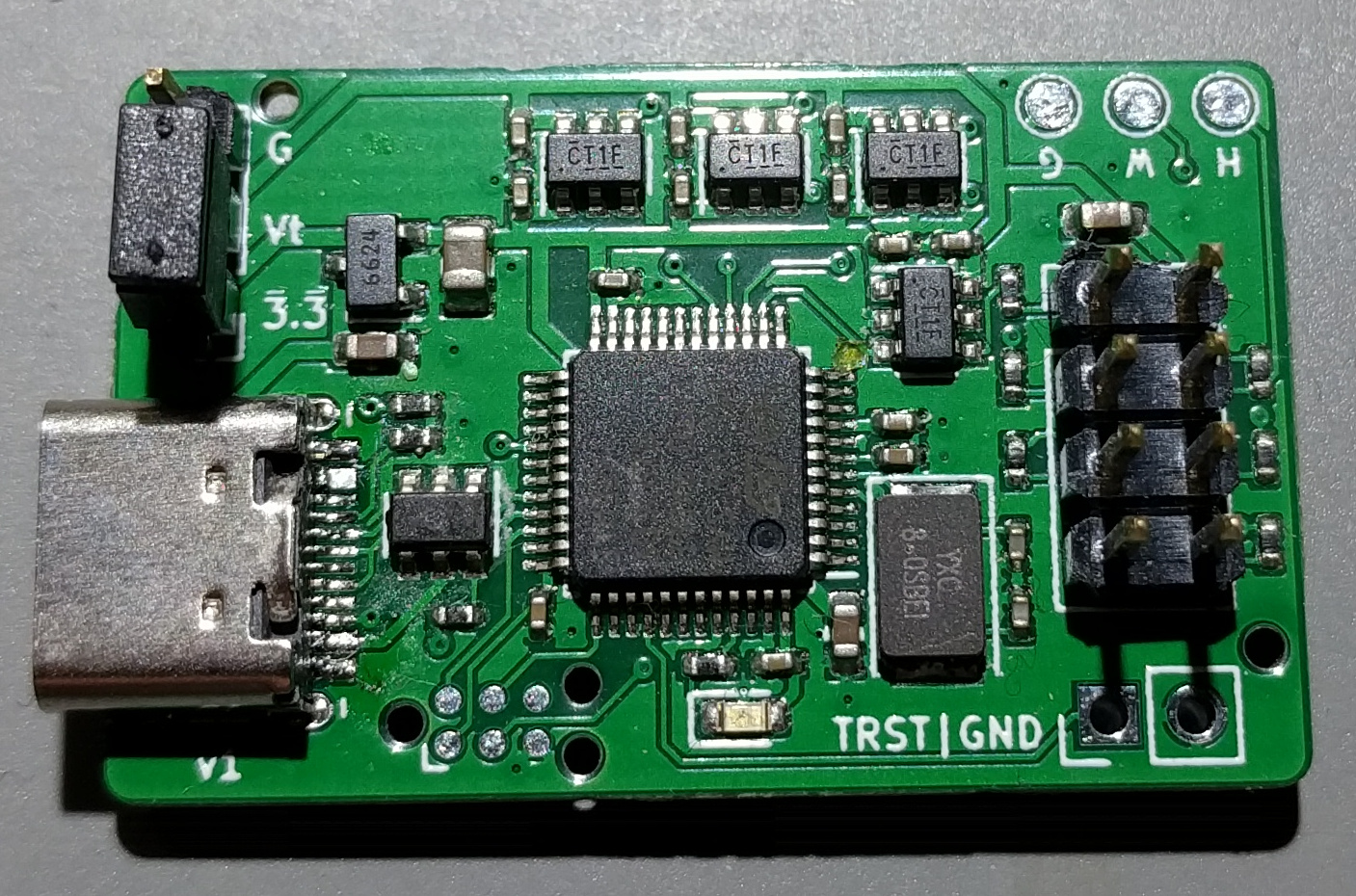
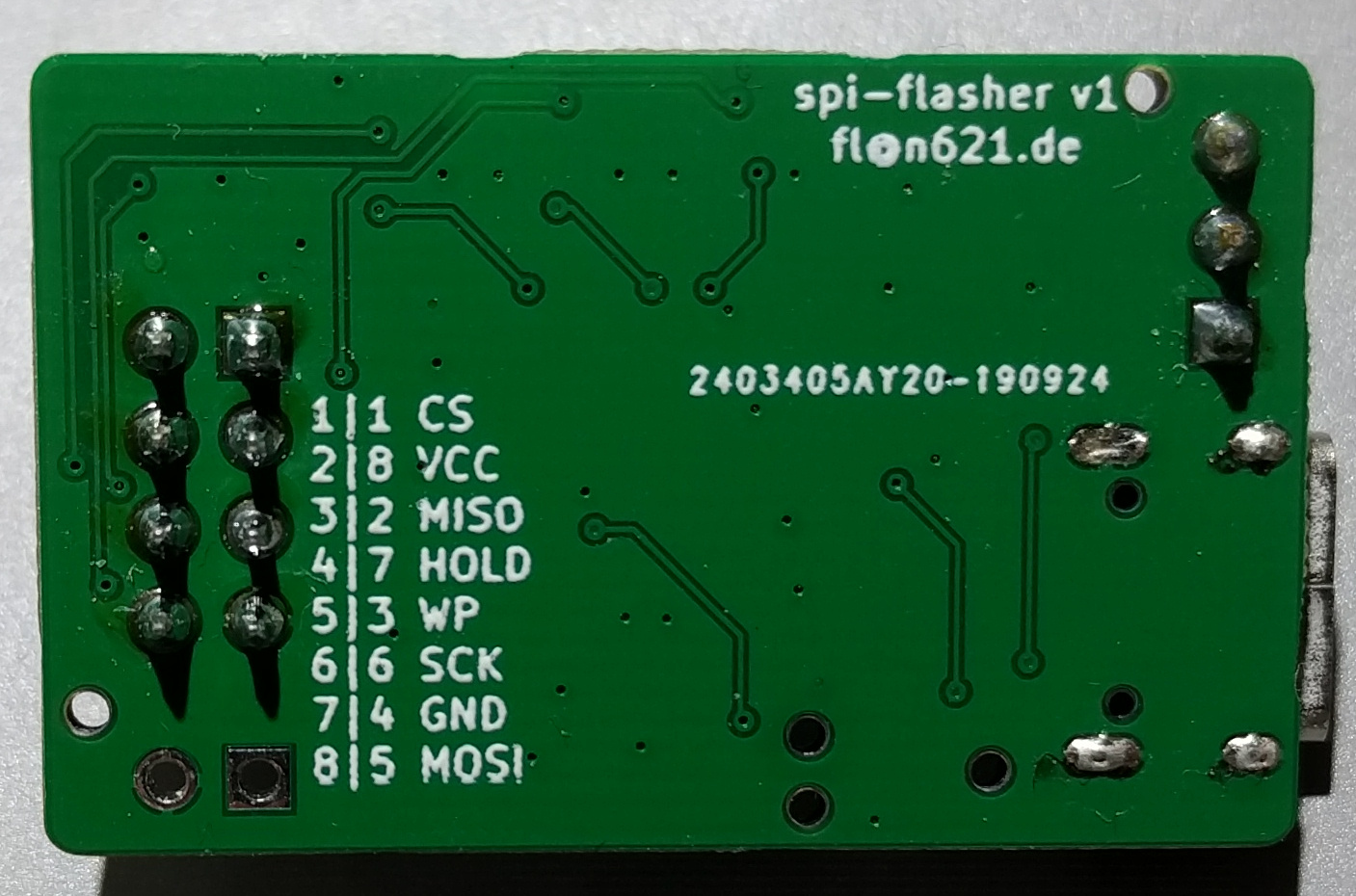
This repository contains an USB-C-to-SPI-flash adapter that is compatible with stm32-vserprog and also has integrated level-shifters towards the SPI flash. This was created mainly to try out the JLCPCB assembly service and because there is no convenient way to program 1.8V flash chips with the "Bluepill + mess of wires" setup I was using before. The pinout is arranged such that it matches the common flash test clips.
Furthermore, there is a simple breakout board that flash chips can be directly soldered onto if space in the target device is too tight to use such a clip (this is mainly useful when reverse-engineering third-party hardware).
The respective fab directories contain fabrication data (and in the case of
the adapter, JLCPCB-style assembly data) for the boards. As JLCPCB cannot
populate connectors at this time, those had to be assembled manually:
The way the target is powered can be selected through the pin header above the USB port: The target can be self-powered (no jumper), powered from the internal 3.3V rail (jumper between 3.3 and Vt) or powered externally (supply power between G and Vt).
The TRST/GND connector was meant as an extension that could be used (given a
modified version of stm32-vserprog) to keep a target device in reset while
accessing the flash to prevent interference. However, this does not really work
out mechanically, so it was never used.
Build stm32-vserprog using BOARD=stm32-jz01v20 and flash the firmware via
the TagConnect connector.
| Qty | Value | Footprint | References |
|---|---|---|---|
| 1 | 100n | Capacitor_SMD:C_0402_1005Metric | C1 |
| 1 | Conn_02x04_Odd_Even | Connector_PinSocket_1.00mm:PinSocket_2x04_P1.00mm_Vertical_SMD | J1 |
| 1 | W25Q32JVSS | Package_SO:SOIC-8_5.23x5.23mm_P1.27mm | U1 |
florolf/spi-flasher
USB-C-to-SPI-flash adapter with level shifting, stm32-vserprog compatible


plinkysynth/plinky_public
a public release of the plinky sw and hw


murexrobotics/electrical
Highly integrated electronics design and printed circuit boards (PCBs) for the MATE ROV Competition. Attempt the impossible.


KaiPereira/Overglade-Badges
NFC hackathon badges for the Overglade game jam in Singapore!

efabless/foss-asic-tools
FOSS-ASIC-TOOLS is all in one container for SKY130 based design both Analog and Digital. Below is a list of the current tools already installed and ready to use.

NikodemBartnik/StarTrckr
Open source star tracker for deep sky astrophotography
It measures 11 × 8 mm and has 2 copper layers, 1.6 mm thick.
3 parts, built around the W25Q32JVSSIQ. The full list of its parts is on this page, with links to each part's symbol and footprint where PCBKit's library has them.
From the florolf/spi-flasher repository on GitHub, at the commit this page was made from: the board is breakout/so8.kicad_pcb. PCBKit opens the board in the browser, with nothing to install.
Its repository publishes it under the CC-BY-SA-4.0 licence: you may reuse it on that licence's terms (keep the author's notice, and for a copyleft licence share your changes alike).