
2 layers104.9 × 75.2 mm
 f0gger/Snes-Ctr
KiCad hardware design files for a custom Super Nintendo Entertainment System (SNES) controller built around the ATmega328P microcontroller, with I²C communication for interfacing with external devices.
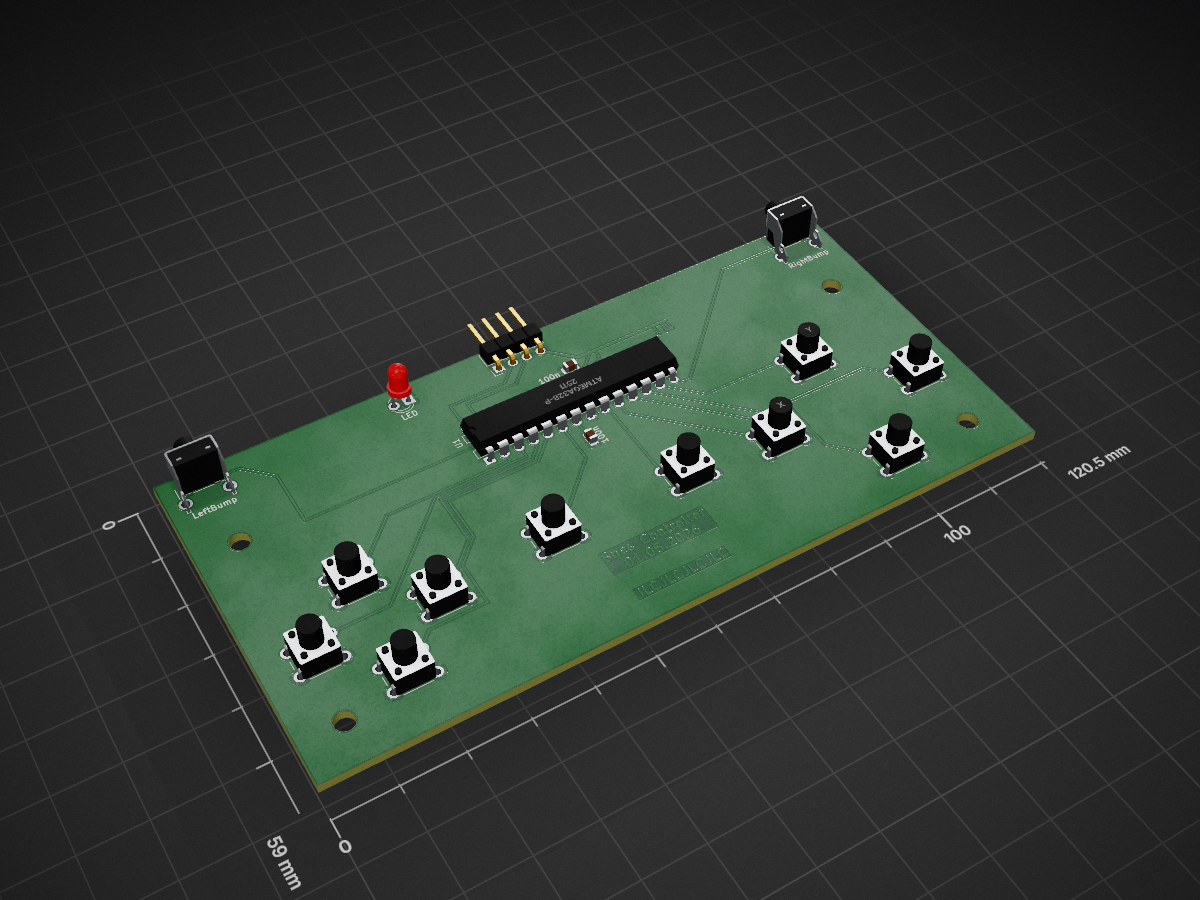
Snes Ctr is an open-source printed circuit board by f0gger, from the f0gger/Snes-Ctr repository on GitHub. It is a 2-layer board of 120.5 × 59 mm with 25 parts on 27 nets, routed with 111 tracks and 4 vias.
It is built around the ATMEGA328-PU. It belongs with the retro computing and games boards and the AVR (ATmega, ATtiny) boards of this library.
KiCad hardware design files for a custom Super Nintendo Entertainment System (SNES) controller built around the ATmega328P microcontroller, with I²C communication for interfacing with external devices.
Snes-Ctr/
├── gerbers/ - Gerber and drill files for PCB manufacturing.
│   ├── Snes-Ctr-B_Cu.gbl
│   ├── Snes-Ctr-B_Mask.gbs
│   ├── Snes-Ctr-B_Paste.gbp
│   ├── Snes-Ctr-B_Silkscreen.gbo
│   ├── Snes-Ctr-Edge_Cuts.gm1
│   ├── Snes-Ctr-F_Cu.gtl
│   ├── Snes-Ctr-F_Mask.gts
│   ├── Snes-Ctr-F_Paste.gtp
│   ├── Snes-Ctr-F_Silkscreen.gto
│   ├── Snes-Ctr-NPTH.drl
│   ├── Snes-Ctr-PTH.drl
│   └── Snes_Ctr_gerbers.zip
├── Snes-Ctr.kicad_dru - Custom PCB design rules
├── Snes-Ctr.kicad_pcb - PCB layout.
├── Snes-Ctr.kicad_pro - KiCad project configuration.
├── Snes-Ctr.kicad_sch - Circuit schematic.
└── README.md
File names and structure may vary depending on the actual project files. Hardware Overview
The controller uses the ATmega328P to interface with the SNES controller inputs and handle communication with external hardware over the I²C bus.
The KiCad project contains the circuit schematic and PCB design, providing a starting point for reviewing, modifying, and manufacturing the hardware. Requirements
KiCad — for viewing and editing the schematic and PCB
ATmega328P-compatible programming hardware — for flashing firmware, if applicableClone this repository:
git clone <repository-url>
cd <repository-directory>
Open the .kicad_pro file in KiCad.
Review the schematic (.kicad_sch) to understand the circuit.
Open the PCB editor to inspect or modify the board layout.
Run the electrical rules check (ERC) and design rules check (DRC) before manufacturing.Before ordering or assembling the PCB:
- Verify the schematic and PCB design.
- Check component footprints and pin assignments.
- Run ERC and DRC in KiCad.
- Generate Gerber files and drill files using KiCad's fabrication tools.
- Confirm the bill of materials (BOM) and component availability.| Qty | Value | Footprint | References |
|---|---|---|---|
| 2 | 100n | Capacitor_SMD:C_0805_2012Metric | 100n, 100n |
| 2 | 4.7k | Resistor_SMD:R_0805_2012Metric | 4.7k, 4.7k |
| 1 | 10k | Resistor_SMD:R_0805_2012Metric | 10k |
| 1 | 680 | Resistor_SMD:R_0805_2012Metric | 680 |
| 1 | A | Button_Switch_THT:SW_PUSH_6mm_H7.3mm | A |
| 1 | ATmega328-P | Package_DIP:DIP-28_W7.62mm | U1 |
| 1 | B | Button_Switch_THT:SW_PUSH_6mm_H7.3mm | B |
| 1 | Conn_01x04_Pin | Connector_PinHeader_2.54mm:PinHeader_1x04_P2.54mm_Horizontal | VCC SDA SCL GND |
| 1 | Down | Button_Switch_THT:SW_PUSH_6mm_H7.3mm | Down |
| 1 | LED | LED_THT:LED_D3.0mm | LED |
| 1 | Left | Button_Switch_THT:SW_PUSH_6mm_H7.3mm | Left |
| 1 | Left Bumper | Button_Switch_THT:SW_Tactile_SPST_Angled_PTS645Vx58-2LFS | LeftBump |
| 1 | Right | Button_Switch_THT:SW_PUSH_6mm_H7.3mm | Right |
| 1 | Right Bumper | Button_Switch_THT:SW_Tactile_SPST_Angled_PTS645Vx58-2LFS | RightBump |
| 1 | Select | Button_Switch_THT:SW_PUSH_6mm_H7.3mm | Select |
| 1 | Start | Button_Switch_THT:SW_PUSH_6mm_H7.3mm | Start |
| 1 | Up | Button_Switch_THT:SW_PUSH_6mm_H7.3mm | Up |
| 1 | X | Button_Switch_THT:SW_PUSH_6mm_H7.3mm | X |
| 1 | Y | Button_Switch_THT:SW_PUSH_6mm_H7.3mm | Y |
The 21 most common of 25 parts.
It measures 120.5 × 59 mm and has 2 copper layers, 1.6 mm thick.
25 parts, built around the ATMEGA328-PU. The full list of its parts is on this page, with links to each part's symbol and footprint where PCBKit's library has them.
From the f0gger/Snes-Ctr repository on GitHub, at the commit this page was made from: the board is Snes-Ctr.kicad_pcb and its schematic Snes-Ctr.kicad_sch. PCBKit opens the board in the browser, with nothing to install.
Its repository states no licence, so its author keeps all rights: ask f0gger before reusing the design.


peej/lumberjack-keyboard
5x12 ortholinear through-hole component keyboard PCB for standard 60% cases

peterheinrich/InternetOverSpaghetti
Transmitting IP packages over a pair of spaghetti thus demonstrating how media independent IP really is.

