4 layers82.4 × 53.3 mm
Sara rx ab
ldab/SARA-Rx-application-board
SARA-R4 NB-IoT + Cat-M1 + GNSS application board - NINA-B3 with Secure MQTT
133 partsMIT
 EthanKahn08/example-pcb
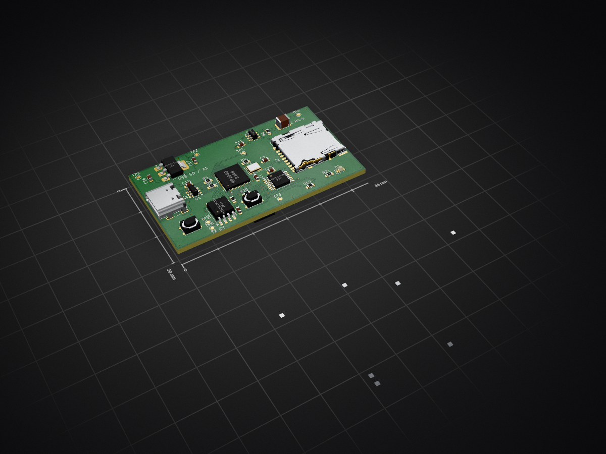
Design-stage RP2040 USB-C microSD reader: KiCad hardware, verification evidence, UART bring-up firmware, and assembly plan. Unbuilt and untested.
Stitch candidate is an open-source printed circuit board by EthanKahn08, from the EthanKahn08/example-pcb repository on GitHub. It is a 4-layer board of 55 × 30 mm with 68 parts on 68 nets, routed with 610 tracks and 84 vias.
It is built around the RP2040, 74LVC125APW and W25Q16JVSSIQ, with the TLV1117LV33DCYR, PESD5V0U2BT and USBLC6-2SC6 among its other parts. Its parts include 23 capacitors, 21 resistors, 6 diodes, 5 ICs and 3 connectors. It belongs with the interfaces and adapters boards and the RP2040 boards of this library.


A custom RP2040 board intended to expose a removable microSD card as a USB drive. It uses 2 MiB external firmware flash, a 12 MHz crystal, USB-C, and a switched SPI card interface.
Status: design stage. No board has been assembled or bench tested. Hardware file checks pass. UART bring-up firmware is included; SD and USB Mass Storage firmware still need implementation.
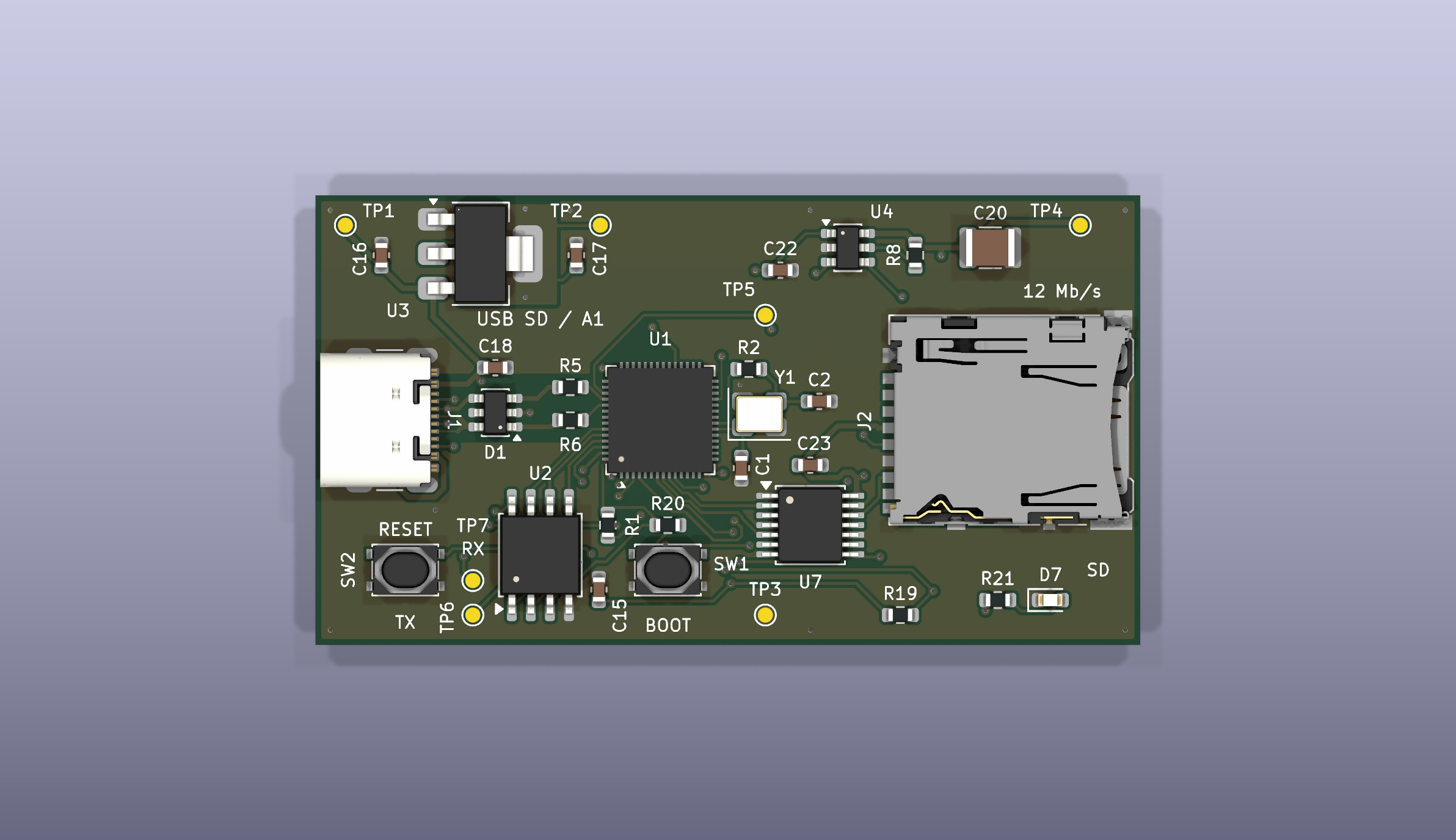
The external flash stores firmware. User files would live on the removable card, with the host owning its filesystem while USB storage is active.
The root A1 files were checked with KiCad 10.0.6 on 2026-10-01 after correcting the issues found in the initial review.
| Check | Result |
|---|---|
| ERC, including footprint filters | 0 errors, 0 warnings |
| DRC, zone refill, and schematic parity | 0 findings; 0 unrouted connections |
| Additional strict checks | 0 findings; no ignored checks |
| Independent schematic / PCB / BOM audit | 68 components and 255 electrical pad instances agree |
| Manufacturing export comparison | All 13 Gerber/drill files match fresh exports apart from timestamps |
| Drills and placements | 93 drill features and 60 fitted placements match native geometry |
Current check logs, publication changes, and the original review provide the evidence and limits. The firmware build record is included with the current evidence.
These results establish file consistency and selected design rules. USB signal quality, enumeration, storage behavior, connector fit, current, temperature, and suspend behavior still need physical tests. The documented USB reference-plane discontinuities remain an open prototype qualification issue; there is no controlled-impedance or compliance claim.
| Location | Purpose |
|---|---|
example.kicad_pro | Open the root A1 project in KiCad |
| Schematic PDF | Read the circuit without KiCad |
| Grouped BOM | Planned exact parts and per-board quantities |
exports/fabrication/ | Refreshed prototype Gerbers and drills |
| Bring-up firmware | Buildable UART diagnostics; card power stays off |
| Storage firmware contract | Pin mapping and planned SD/USB behavior |
| Parts and assembly plan | What to buy, fabrication review, and first power-on |
| Reproduction | Repeat the checks and exports |
The local libraries resolve through ${KIPRJMOD}. Standard KiCad 10 models are needed for the 3D view. revisions/A2/ is an archived preparation workspace, not a completed revision. work/ contains historical generation scripts and intermediate layouts; regenerating can overwrite reviewed routing.
An enclosure and debug fixture have not been designed. The RP2040 exposed-pad QFN needs reflow assembly.
The project uses scripted generation, local autorouting, and AI-assisted drafting and review. Library sources and terms identify upstream material. Original work has no broader reuse license selected; the included KiCad library collection retains its upstream license.
| Qty | Value | Footprint | References |
|---|---|---|---|
| 14 | 100nF | Device:Capacitor_SMD__C_0603_1608Metric | C3, C4, C5, C6, C7, C8, C9, C10, C13, C14, C15, C18, C21, C23 |
| 5 | 47k | Device:Resistor_SMD__R_0603_1608Metric | R12, R13, R14, R15, R16 |
| 4 | 1k | Device:Resistor_SMD__R_0603_1608Metric | R2, R8, R20, R21 |
| 4 | 1uF | Device:Capacitor_SMD__C_0603_1608Metric | C11, C12, C16, C22 |
| 4 | PESD5V0U2BT | Device:Package_TO_SOT_SMD__SOT-23 | D2, D4, D5, D6 |
| 3 | 10k | Device:Resistor_SMD__R_0603_1608Metric | R1, R18, R19 |
| 3 | 33 | Device:Resistor_SMD__R_0603_1608Metric | R9, R10, R11 |
| 2 | 100k | Device:Resistor_SMD__R_0603_1608Metric | R7, R17 |
| 2 | 15pF | Device:Capacitor_SMD__C_0603_1608Metric | C1, C2 |
| 2 | 27 | Device:Resistor_SMD__R_0603_1608Metric | R5, R6 |
| 2 | 5.1k | Device:Resistor_SMD__R_0603_1608Metric | R3, R4 |
| 1 | 12MHz CL10pF | Device:Crystal__Crystal_SMD_3225-4Pin_3.2x2.5mm | Y1 |
| 1 | 1V1 | Device:TestPoint__TestPoint_Pad_D1.0mm | TP5 |
| 1 | 3V3 | Device:TestPoint__TestPoint_Pad_D1.0mm | TP2 |
| 1 | 4.7nF | Device:Capacitor_SMD__C_0603_1608Metric | C19 |
| 1 | 4.7uF | Device:Capacitor_SMD__C_0603_1608Metric | C17 |
| 1 | 47uF | Device:Capacitor_SMD__C_1210_3225Metric | C20 |
| 1 | 74LVC125APW | Device:Package_SO__TSSOP-14_4.4x5mm_P0.65mm | U7 |
| 1 | BOOT | Device:Button_Switch_SMD__SW_SPST_PTS810 | SW1 |
| 1 | GND | Device:TestPoint__TestPoint_Pad_D1.0mm | TP3 |
| 1 | GREEN | Device:LED_SMD__LED_0603_1608Metric | D7 |
| 1 | RESET | Device:Button_Switch_SMD__SW_SPST_PTS810 | SW2 |
| 1 | RP2040 | Device:Package_DFN_QFN__QFN-56-1EP_7x7mm_P0.4mm_EP3.2x3.2mm | U1 |
| 1 | SD_3V3 | Device:TestPoint__TestPoint_Pad_D1.0mm | TP4 |
| 1 | SWD pads | Device:custom__SWD_1x05_Pads | J3 |
| 1 | TLV1117LV33DCYR | Device:Package_TO_SOT_SMD__SOT-223-3_TabPin2 | U3 |
| 1 | TPS22918DBVR | Device:Package_TO_SOT_SMD__SOT-23-6 | U4 |
| 1 | UART_RX | Device:TestPoint__TestPoint_Pad_D1.0mm | TP7 |
| 1 | UART_TX | Device:TestPoint__TestPoint_Pad_D1.0mm | TP6 |
| 1 | USB-C USB2 | Device:Connector_USB__USB_C_Receptacle_GCT_USB4105-xx-A_16P_TopMnt_Horizontal | J1 |
| 1 | USBLC6-2SC6 | Device:Package_TO_SOT_SMD__SOT-23-6 | D1 |
| 1 | VBUS | Device:TestPoint__TestPoint_Pad_D1.0mm | TP1 |
| 1 | W25Q16JVSSIQ | Device:Package_SO__SOIC-8_5.3x5.3mm_P1.27mm | U2 |
| 1 | microSD / detect | Device:Connector_Card__microSD_HC_Hirose_DM3AT-SF-PEJM5 | J2 |
It measures 55 × 30 mm and has 4 copper layers, 1.6 mm thick.
68 parts, built around the RP2040, 74LVC125APW, W25Q16JVSSIQ and TLV1117LV33DCYR. The full list of its parts is on this page, with links to each part's symbol and footprint where PCBKit's library has them.
From the EthanKahn08/example-pcb repository on GitHub, at the commit this page was made from: the board is work/stitch-candidate.kicad_pcb and its schematic card-protection.kicad_sch. PCBKit opens the board in the browser, with nothing to install.
Its repository states no licence, so its author keeps all rights: ask EthanKahn08 before reusing the design.
ldab/SARA-Rx-application-board
SARA-R4 NB-IoT + Cat-M1 + GNSS application board - NINA-B3 with Secure MQTT

picorubykaigi/adventure-board-pcb
PicoRubyKaigi 2026 の オリジナルRP2350 基板「Adventure Board」の設計データ(KiCad 9)

elcruzo/learned-pcb-placement
GNN-guided simulated annealing for PCB component placement. We train a Graph Attention Network on SA rollout data to learn which components to move and where, then use these predictions to bias the SA search.

RandBeyy/Standalone_AVR_Programmer
A standalone, SD card based programmer for AVR microcontrollers. The device is built around an ATmega328P and programs a target without requiring a computer during normal use.


