Skip to the content
PCBKitNew board
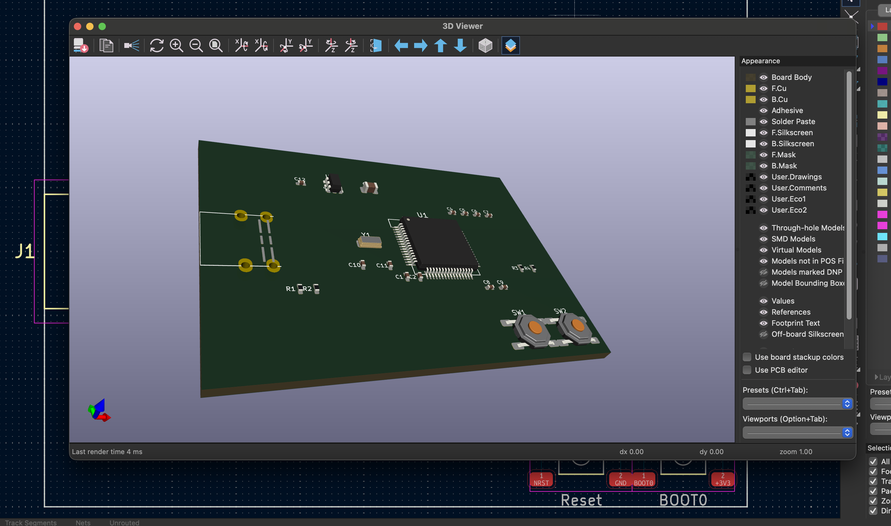
4 layers55 × 40 mmStm32 usbc board, the printed circuit board in 3D

Stm32 usbc board

enishyseni/pcbdesign

A KiCad 8 circuit board project for an STM32F405RGT6-based development board with USB-C connectivity.

Size
55 × 40 mm
Copper layers
4
Thickness
1.6 mm
Parts
22
Nets
15
Pads
131
Tracks, vias
0, 0
Routed
Not yet
KiCad
KiCad 8.0 (file 20240108)
Created
15 Mar 2026
Updated
15 Mar 2026

Overview

Stm32 usbc board is an open-source printed circuit board by enishyseni, from the enishyseni/pcbdesign repository on GitHub. It is a 4-layer board of 55 × 40 mm with 22 parts on 15 nets.

It is built around the STM32F405RGT6 and AP2112K-3.3. Its parts include 12 capacitors, 4 resistors, 2 ICs, 2 switches and 1 connector. It belongs with the STM32 boards of this library.

Main components

2

README

README.md

STM32F405RGT6 USB-C Development Board

A KiCad 8 circuit board project for an STM32F405RGT6-based development board with USB-C connectivity.

Screenshots

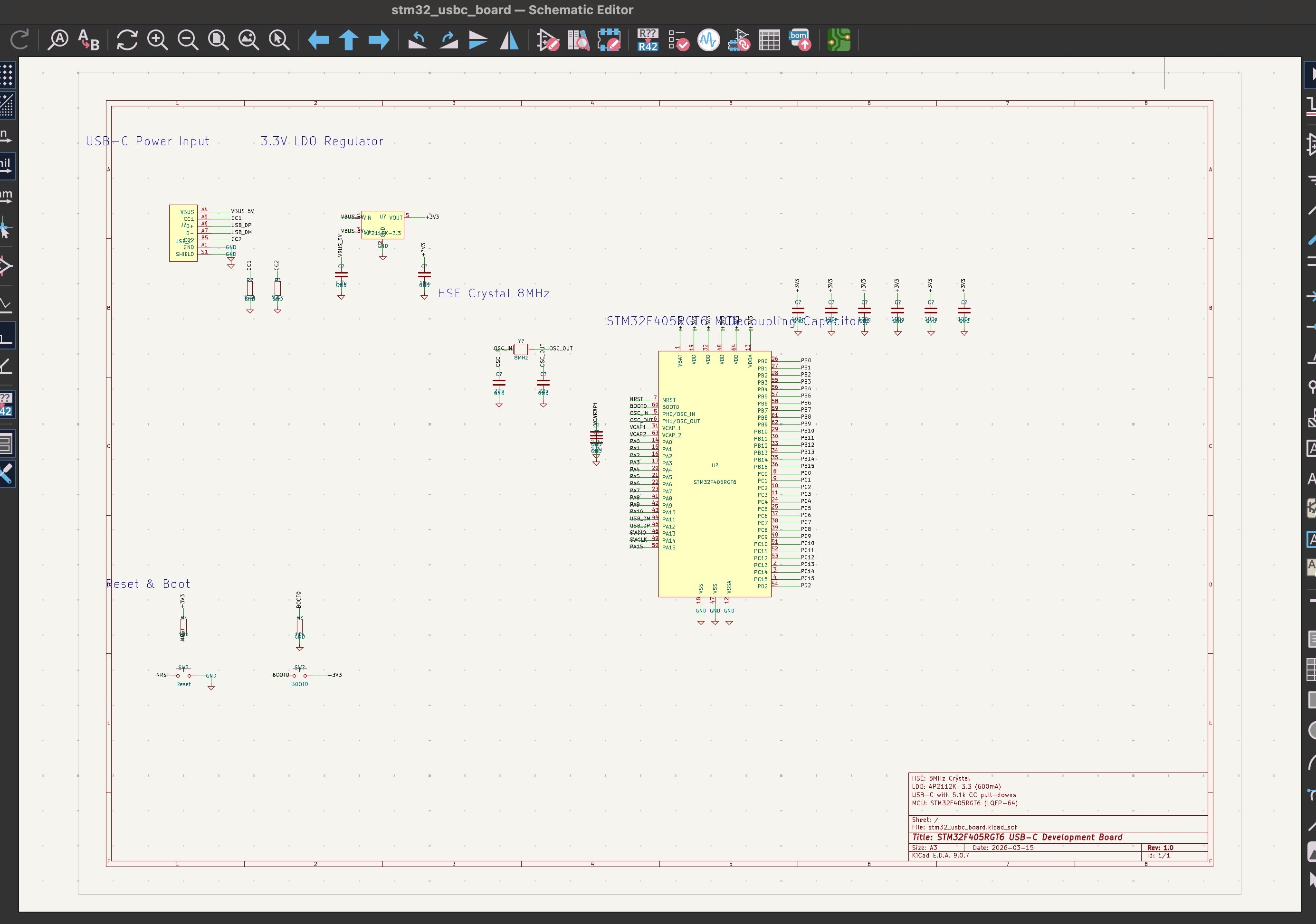
Schematic

Schematic

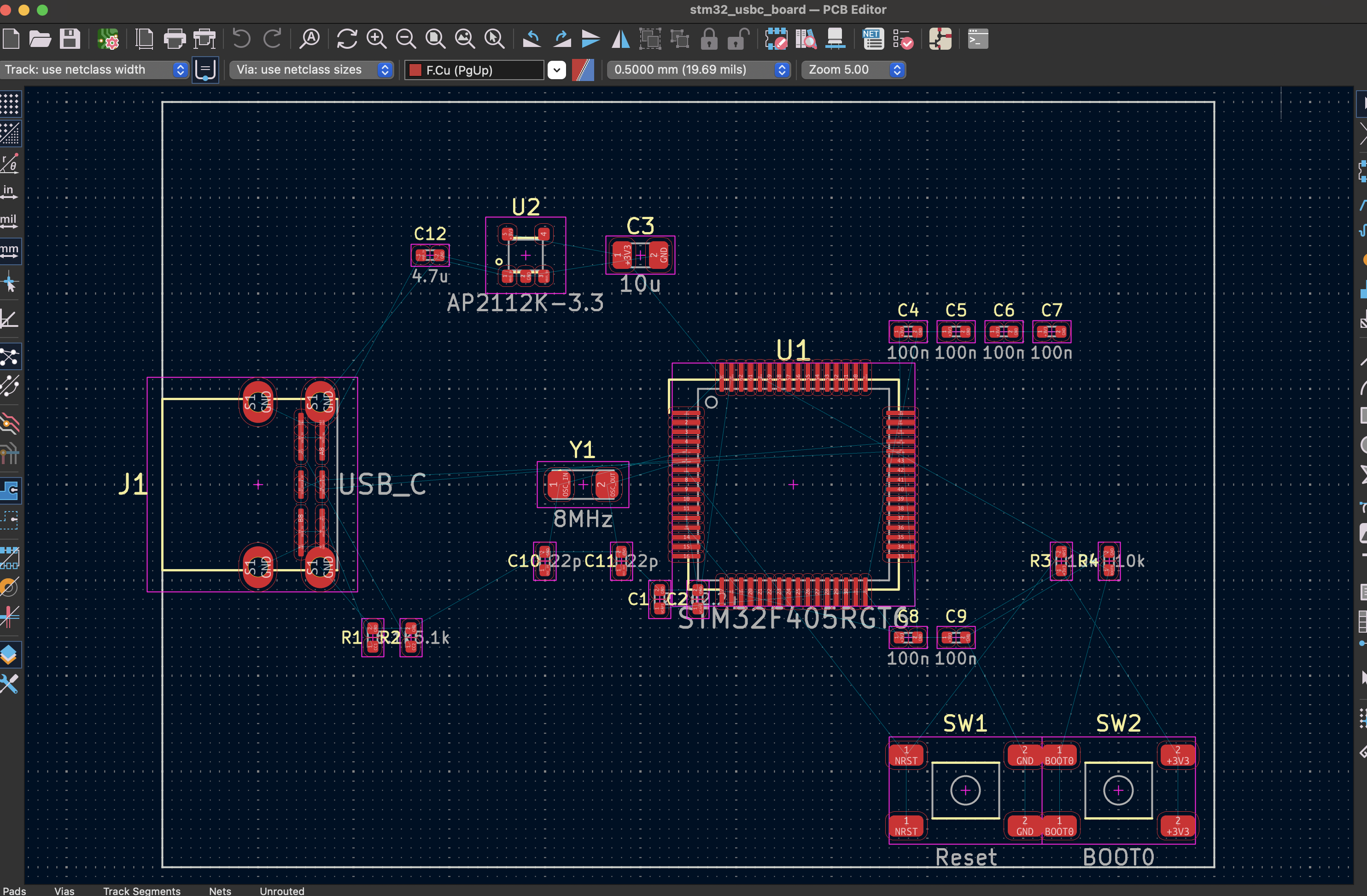
PCB Layout

PCB Layout

3D View

3D View

Circuit Overview

text
USB-C (5V) ──► AP2112K-3.3 LDO ──► 3.3V Rail ──► STM32F405RGT6
   │                                                    │
   ├── D+/D- ──────────────────────────── PA12/PA11 (USB OTG FS)
   ├── CC1 ── 5.1kΩ ── GND                             │
   └── CC2 ── 5.1kΩ ── GND              8MHz Crystal ── PH0/PH1 (HSE)
                                                        │
                                         NRST ── 10kΩ ── 3V3 + Reset Button
                                         BOOT0 ── 10kΩ ── GND + Boot Button

Project Files

FileDescription
stm32_usbc_board.kicad_proKiCad project settings (4-layer PCB, net classes)
stm32_usbc_board.kicad_schComplete schematic with all components wired
stm32_usbc_board.kicad_pcbPCB layout template (40×30mm, 4-layer stackup)
sym-lib-tableSymbol library references (KiCad standard libs)
fp-lib-tableFootprint library references (KiCad standard libs)
BOM.csvFull Bill of Materials with MPNs and supplier info
generate_schematic.pyPython script to regenerate the schematic

Bill of Materials (20 components)

Active Components

RefValuePackageDescription
U1STM32F405RGT6LQFP-64ARM Cortex-M4 MCU, 168MHz, 1MB Flash, USB OTG
U2AP2112K-3.3SOT-23-5600mA LDO Regulator, 3.3V Fixed Output

Connectors

RefValuePackageDescription
J1USB-C16-Pin SMDUSB Type-C Receptacle (USB 2.0)

Passive Components — Capacitors

RefValuePackageDescription
C1, C22.2µF0402VCAP1 and VCAP2 (STM32 internal regulator)
C310µF08053.3V bulk decoupling
C4–C9100nF0402VDD/VDDA/VBAT decoupling (×6)
C10, C1122pF0402HSE crystal load capacitors
C124.7µF0402LDO input capacitor

Passive Components — Resistors

RefValuePackageDescription
R1, R25.1kΩ0402USB-C CC1/CC2 pull-down (device mode)
R310kΩ0402NRST pull-up to 3.3V
R410kΩ0402BOOT0 pull-down to GND

Oscillator

RefValuePackageDescription
Y18MHz3215 SMDHSE crystal (required for USB timing)

Switches

RefValuePackageDescription
SW1ResetSMD TactilePulls NRST low to reset MCU
SW2BOOT0SMD TactilePulls BOOT0 high for DFU bootloader

Schematic Net Connections

Power

  • VBUS_5V: USB-C VBUS → LDO VIN, LDO EN (always-on)
  • +3V3: LDO VOUT → All MCU VDD pins, VDDA, VBAT, decoupling caps
  • GND: All ground pins interconnected

USB 2.0 (Full Speed / High Speed)

  • USB_DP (D+): USB-C pin A6 ↔ MCU PA12 (OTG_FS_DP)
  • USB_DM (D-): USB-C pin A7 ↔ MCU PA11 (OTG_FS_DM)
  • CC1: USB-C pin A5 → 5.1kΩ → GND (identifies as UFP/device)
  • CC2: USB-C pin B5 → 5.1kΩ → GND

Clock

  • OSC_IN: Crystal pin 1 ↔ MCU PH0, with 22pF load cap to GND
  • OSC_OUT: Crystal pin 2 ↔ MCU PH1, with 22pF load cap to GND

Control

  • NRST: MCU reset pin, 10kΩ pull-up to 3.3V, SW1 pulls to GND
  • BOOT0: MCU boot select, 10kΩ pull-down to GND, SW2 pulls to 3.3V
  • SWDIO/SWCLK: Exposed on PA13/PA14 for SWD debug

Internal Regulation

  • VCAP1: MCU pin 31 → 2.2µF → GND
  • VCAP2: MCU pin 63 → 2.2µF → GND

PCB Layout Notes

Recommended Stack-up (4-layer)

  1. F.Cu — Signal + components
  2. In1.Cu — GND plane
  3. In2.Cu — 3.3V power plane
  4. B.Cu — Signal + components

Layout Guidelines

  • Place decoupling caps (C4–C9) as close as possible to each MCU VDD pin
  • Keep crystal (Y1) and load caps (C10, C11) within 5mm of PH0/PH1 pins
  • Route USB D+/D- as a 90Ω differential pair (for USB HS; less critical for FS)
  • Place VCAP caps (C1, C2) directly adjacent to VCAP1/VCAP2 pins
  • USB-C connector on board edge with GND stitching vias nearby
  • Keep analog ground (VSSA) clean with separate return path if possible

Design Rules

  • Min track width: 0.2mm (signal), 0.5mm (power)
  • Min clearance: 0.2mm
  • Via: 0.6mm pad / 0.3mm drill
  • Board outline: 40mm × 30mm (adjustable)

Getting Started

Prerequisites

  • KiCad 8.0+
  • Standard KiCad libraries installed (included with default KiCad installation)

Opening the Project

  1. Open KiCad 8
  2. File → Open Project → Select stm32_usbc_board.kicad_pro
  3. The schematic editor will show the full circuit
  4. Use Tools → Update PCB from Schematic to import components to the PCB

Regenerating the Schematic

If you modify the circuit design:

bash
python3 generate_schematic.py

This regenerates stm32_usbc_board.kicad_sch from the Python source.

Generating Fabrication Files

  1. Open the PCB editor
  2. File → Fabrication Outputs → Gerbers → Output to fabrication/
  3. File → Fabrication Outputs → Drill Files → Same directory
  4. Zip the fabrication/ folder for your PCB manufacturer

Programming the Board

Via USB-C (DFU Bootloader)

  1. Hold SW2 (BOOT0) while pressing SW1 (Reset)
  2. Release Reset, then release BOOT0
  3. MCU enters built-in DFU bootloader on USB
  4. Use dfu-util or STM32CubeProgrammer to flash firmware

Via SWD (Debug Probe)

Connect an ST-Link or J-Link to the SWD pins:

  • SWDIO → PA13
  • SWCLK → PA14
  • GND → Any GND pin
  • 3V3 → Any 3.3V pin (for target detection)

Crystal Load Capacitor Calculation

For an 8MHz crystal with specified load capacitance $C_L$:

$$C_{load} = 2 \times (C_L - C_{stray})$$

With $C_L = 20\text{pF}$ and $C_{stray} \approx 5\text{pF}$:

$$C_{load} = 2 \times (20 - 5) = 30\text{pF} \implies 22\text{pF per side (standard value)}$$

The 22pF caps (C10, C11) are suitable for most 8MHz crystals with 18–20pF load spec.

License

This hardware design is provided as-is for educational and development purposes.

Parts

22
QtyValueFootprintReferences
6100nCapacitor_SMD:C_0402_1005MetricC4, C5, C6, C7, C8, C9
210kResistor_SMD:R_0402_1005MetricR3, R4
22.2uCapacitor_SMD:C_0402_1005MetricC1, C2
222pCapacitor_SMD:C_0402_1005MetricC10, C11
25.1kResistor_SMD:R_0402_1005MetricR1, R2
110uCapacitor_SMD:C_0805_2012MetricC3
14.7uCapacitor_SMD:C_0402_1005MetricC12
18MHzCrystal:Crystal_SMD_3215-2Pin_3.2x1.5mmY1
1AP2112K-3.3Package_TO_SOT_SMD:SOT-23-5U2
1BOOT0Button_Switch_SMD:SW_SPST_TL3342SW2
1ResetButton_Switch_SMD:SW_SPST_TL3342SW1
1STM32F405RGT6Package_QFP:LQFP-64_10x10mm_P0.5mmU1
1USB_CConnector_USB:USB_C_Receptacle_HRO_TYPE-C-31-M-12J1

Questions

How big is the Stm32 usbc board PCB?

It measures 55 × 40 mm and has 4 copper layers, 1.6 mm thick.

What parts does the Stm32 usbc board use?

22 parts, built around the STM32F405RGT6 and AP2112K-3.3. The full list of its parts is on this page, with links to each part's symbol and footprint where PCBKit's library has them.

Where can I download the Stm32 usbc board KiCad files?

From the enishyseni/pcbdesign repository on GitHub, at the commit this page was made from: the board is stm32_usbc_board.kicad_pcb and its schematic stm32_usbc_board.kicad_sch. PCBKit opens the board in the browser, with nothing to install.

Can I use the Stm32 usbc board design in my own project?

Its repository states no licence, so its author keeps all rights: ask enishyseni before reusing the design.

Similar boards

  • 4 layers36 × 36 mmRl fc f405.routed, the printed circuit board in 3D

    Rl fc f405.routed

    GabuGravin41/rlpcb

    RL PCB sits beside KiCad and works like a senior hardware engineer looking over your shoulder. You describe what you want to build; it helps you choose real parts from your KiCad libraries, works out the values, places…

    65 parts2
  • 4 layers70 × 100 mmSkylink fc, the printed circuit board in 3D

    Skylink fc

    ajisrawi/5g-3d-printed-drone

    3D-printed quadcopter with a custom F405 flight controller, 4G/5G companion connectivity, and phone control

    136 parts
  • 4 layers58.7 × 35.5 mmMeowCU, the printed circuit board in 3D

    MeowCU

    eggsacc/pcb-MeowCU

    4-layer STM32F405RGT6 MeowCU 🐱 (MCU) dev module with commonly used peripherals broken out for easy access, and a dedicated CAN transceiver. Also includes 2 user programmable buttons and mini OLED display.

    69 parts
  • 4 layers50 × 50 mmFC PROTOTYPE, the printed circuit board in 3D

    FC PROTOTYPE

    Harihara0309/Flightcontroller_PCB_design

    88 parts
  • 4 layers36.9 × 36.9 mmFpv flight controller, the printed circuit board in 3D

    Fpv flight controller

    stefanpopovic-dev/fpv-flight-controller

    An open-hardware, 4-layer FPV flight controller board built around the STM32F405RGT6, designed in KiCad. Currently at hardware revision REV3. Designed to run Betaflight.

    111 partsCERN-OHL-S-2.0
  • 2 layers59.1 × 99.9 mmCheap FOCer 2 60mm, the printed circuit board in 3D

    Cheap FOCer 2 60mm

    shamansystems/Cheap-FOCer-2

    Low-Cost Motor Controller based on the VESC 6

    193 parts407
  • 4 layers55 × 55 mmRBoard, the printed circuit board in 3D

    RBoard

    pms67/LittleBrain-STM32F4-Sensorboard

    STM32F4-based PCB interfacing with a variety of sensors.

    90 parts339
  • 4 layers75.2 × 99.5 mmFOC, the printed circuit board in 3D

    FOC

    nordstream3/FOC

    Date | Manufacturer | amount | includes | shipping & tax | price | -------- | -------- | -------- | -------- | -------- | -------- | 2024-01-17 | JLCPCB | 10 boards | All assembled excl fets and caps | YES, to EU |…

    261 parts81