2 layers19.1 × 31.8 mm

 emeb/spi_fiend17
STM32F042-based USB to SPI device for programming iCE40 FPGAs
Spi fiend is an open-source printed circuit board by emeb, from the emeb/spi_fiend repository on GitHub, published under the MIT licence. It is a 4-layer board of 34.8 × 18 mm with 28 parts on 37 nets, routed with 279 tracks and 46 vias.
It is built around the STM32F042G6U6 and DRTR5V0U4S. Its parts include 9 resistors, 5 capacitors, 5 connectors, 3 ICs and 3 diodes. It belongs with the fPGA and programmable logic and interfaces and adapters boards and the STM32 boards of this library.


STM32F042-based USB to SPI device for programming iCE40 FPGAs
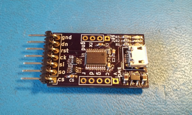
Most open-source projects that use Lattice iCE40 FPGAs rely on the FTDI FT2232 High-speed UART/FIFO chip to provide a SPI interface for programming the FPGA and SPI Flash chip which contains the bitstream for self-configuration at power-up. I've got nothing against FTDI, but the chips are big, require a crystal and are fairly expensive in DIY quantities. On top of that I've been using STM32 for years and have been looking for an excuse to dig into some more USB applications so a USB to SPI bridge seemed like a good place to start.
This device uses the small and inexpensive STM32F042F6P6 in a 20-pin TSSOP package. It supports crystal-less USB operation by syncing its internal RC oscillator to the USB SOF signal and has enough SRAM and Flash to support a moderately complex feature set:
To build this you will need the following tools:
The board design is available in the 'hardware' directory. The Kicad PCB can be submitted directly to OSHpark.com, or traditional Gerbers can be exported using the application. Part values and packages are noted in the schematic.
Note: in the Revision 1 PCB layout the USB connector doesn't overhang the PCB edge and there is a slight interference with the lower lip. Filing a slight chamfer on the PCB edge under the connector will allow it to sit flush to the board.
The Firmware README has instructions on building the preferred firmware for the SPI Fiend.
The host appliction runs on a Linux PC and communicates with the hardware device via standard USB Serial protocols. Build the host application by changing to the 'host' directory and executing 'make'. The built-in help should provide a guide to available options, but here's a quick list of common actions:
In ordinary operation, the LED nearest the USB connector lights to indicate powerup, the center LED lights when an error is detected during operation and the outer LED lights when programming SPI flash.
Initial commit with hardware, firmware and host application
Updated with dual firmware that supports FPGA, flash and UART
| Qty | Value | Footprint | References |
|---|---|---|---|
| 5 | 1k | Resistor_SMD:R_0402_1005Metric | R1, R2, R3, R4, R5 |
| 3 | 0.1uF | Capacitor_SMD:C_0402_1005Metric | C1, C2, C3 |
| 3 | LED_ALT | LED_SMD:LED_0603_1608Metric | D1, D2, D3 |
| 2 | 5k1 | Resistor_SMD:R_0402_1005Metric | R8, R9 |
| 2 | SW_Push | emeb_library:SW_SPST_PTS815 | SW1, SW2 |
| 1 | 10k | Resistor_SMD:R_0402_1005Metric | R6 |
| 1 | 10uf | Capacitor_SMD:C_0805_2012Metric | C5 |
| 1 | 1M | Resistor_SMD:R_0402_1005Metric | R7 |
| 1 | 1uf | Capacitor_SMD:C_0402_1005Metric | C4 |
| 1 | CONN_01X04 | Connector_PinHeader_2.54mm:PinHeader_1x03_P2.54mm_Vertical | J2 |
| 1 | CONN_01X05 | Connector_PinHeader_2.54mm:PinHeader_1x05_P2.54mm_Vertical | J5 |
| 1 | CONN_01X07 | Connector_PinHeader_2.54mm:PinHeader_1x07_P2.54mm_Vertical | J3 |
| 1 | DRTR5V0U4S | Package_TO_SOT_SMD:SOT-363_SC-70-6 | U2 |
| 1 | PROG HEADER | Connector_PinHeader_1.27mm:PinHeader_2x05_P1.27mm_Vertical_SMD | J4 |
| 1 | STM32F042G6U6 | emeb_library:IC_STM32F042G6U6 | U1 |
| 1 | USB_C_Receptacle_USB2.0 | Connector_USB:USB_C_Receptacle_HRO_TYPE-C-31-M-12 | J1 |
| 1 | Val** | emeb_library:avatar_small | Ref** |
| 1 | XC6222B331MR-G | Package_TO_SOT_SMD:SOT-23-5 | U3 |


emeb/RP2040_Projects
A collection of random projects based on the Raspberry Pi RP2040 MCU


msaribekyan/rx5808-receiver
RX5808 based 5.8 GHz analog video receiver module


It measures 34.8 × 18 mm and has 4 copper layers, 4.69 mm thick.
28 parts, built around the STM32F042G6U6 and DRTR5V0U4S. The full list of its parts is on this page, with links to each part's symbol and footprint where PCBKit's library has them.
From the emeb/spi_fiend repository on GitHub, at the commit this page was made from: the board is hardware/v0.2/spi_fiend.kicad_pcb and its schematic hardware/v0.2/spi_fiend.kicad_sch. PCBKit opens the board in the browser, with nothing to install.
Its repository publishes it under the MIT licence: you may reuse it on that licence's terms (keep the author's notice, and for a copyleft licence share your changes alike).