
2 layers21.1 × 26.9 mm

 Elektropioneer/EP_Module
This repo is used for creating modules for the main board
EP Module Mosfet is an open-source printed circuit board by Elektropioneer, from the Elektropioneer/EP_Module repository on GitHub. It is a 2-layer board of 17.8 × 29.8 mm with 14 parts on 12 nets, routed with 93 tracks and 0 vias.
It is built around the BS170. Its parts include 4 connectors, 3 resistors, 3 diodes, 3 transistors and 1 IC. It belongs with the FPGA and CPLD boards of this library.
This module contains 3xBS170 mosfets.
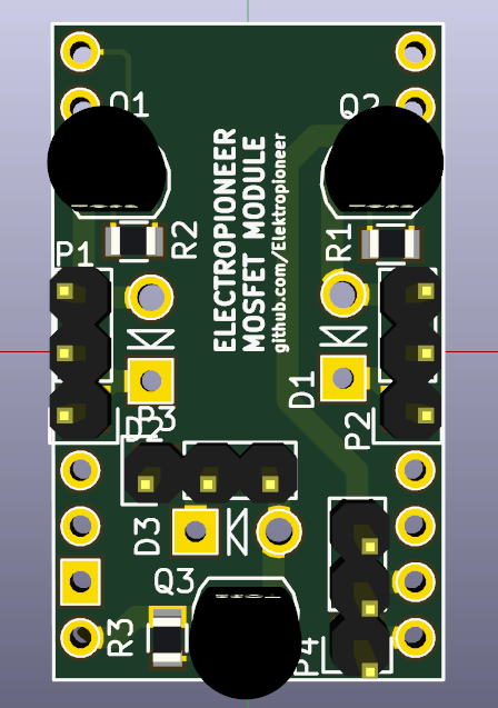
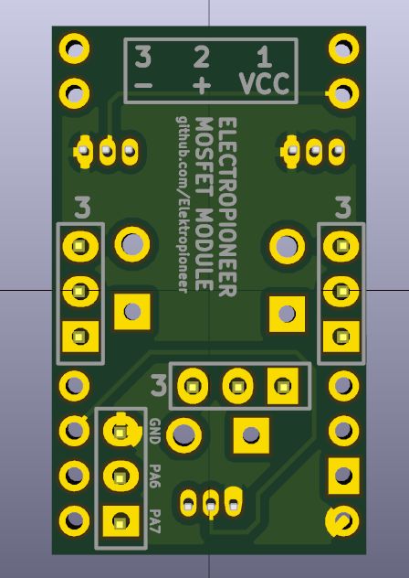
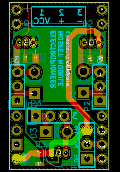
| Qty | Value | Footprint | References |
|---|---|---|---|
| 4 | CONN_01X03 | Pin_Headers:Pin_Header_Straight_1x03 | P1, P2, P3, P4 |
| 3 | BS170 | TO_SOT_Packages_THT:TO-92_Inline_Narrow_Oval | Q1, Q2, Q3 |
| 3 | D | Diodes_ThroughHole:Diode_DO-41_SOD81_Vertical_AnodeUp | D1, D2, D3 |
| 3 | R | Resistors_SMD:R_0805 | R1, R2, R3 |
| 1 | EP_MODULE | EP_Module:EP_Module | U1 |
It measures 17.8 × 29.8 mm and has 2 copper layers, 1.6 mm thick.
14 parts, built around the BS170. The full list of its parts is on this page, with links to each part's symbol and footprint where PCBKit's library has them.
From the Elektropioneer/EP_Module repository on GitHub, at the commit this page was made from: the board is Module_Versions/MOSFET/EP_Module_Mosfet.kicad_pcb. PCBKit opens the board in the browser, with nothing to install.
Its repository states no licence, so its author keeps all rights: ask Elektropioneer before reusing the design.


pablozg/freeds
Derivador de energía solar excedente creado por Pablo Zerón, Diseño PCB por Amcalo, Tester original por Aeizoon, Wiki por Zoilo Mora

PhysicsDptAngers/polyUAnalog
Open source, analog and polyphonic synthesizer


DRWJSCHMIDT/T41
This is the repository for the officially released V10, V11, and V12 versions of the T41 Software Defined Transceiver hardware and kits.

sffubs/dactyl_manuform_gimbal
Instrutions and designs for building the dactyl-manuform-gimbal keyboard