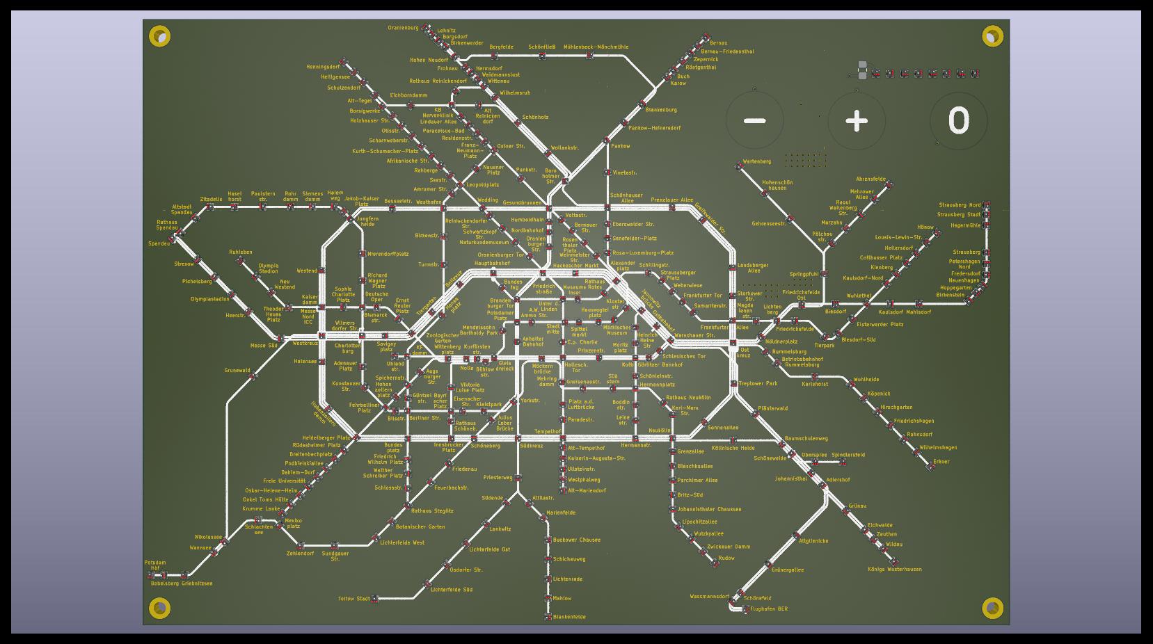
2 layers850.2 × 267.4 mm

 elektrojupp/berlin_bahn
There are some commercial maps of similar design out there. They mostly use multiple LEDs per station and show less complexity by splitting services into separate maps.
Berlin bahn is an open-source printed circuit board by elektrojupp, from the elektrojupp/berlin_bahn repository on GitHub, published under the Apache-2.0 licence. It is a 2-layer board of 153 × 107 mm with 332 parts on 365 nets, routed with 773 tracks and 1,011 vias.
It is built around the ESP32-DEVKITC-32UE, XL-1010RGBC-WS2812B-DZ and 74HC14. Its parts include 325 ICs, 1 capacitor and 1 resistor. It belongs with the ESP32 boards of this library.


There are some commercial maps of similar design out there. They mostly use multiple LEDs per station and show less complexity by splitting services into separate maps.
This project shows the complete maps for Berlin’s suburban rail and subway. It uses 312 NeoPixel-compatible RGB LEDs for 314 stations on a two-layer board. The firmware targets an ESP32-S3 DevKitC-1 N16R8 with 8 MB PSRAM.
The PCB design is done in KiCad 9. It uses SK6805-EC10-000 NeoPixel-compatible LEDs by OPSCO connected in one non-intersecting path.
The LEDs are only 1.1×1.1 mm in size and can be sourced from JLCPCB for PCB manufacturing and assembly.
The current KiCad board is 153×107 mm, roughly the size of a DIN A6 sheet.
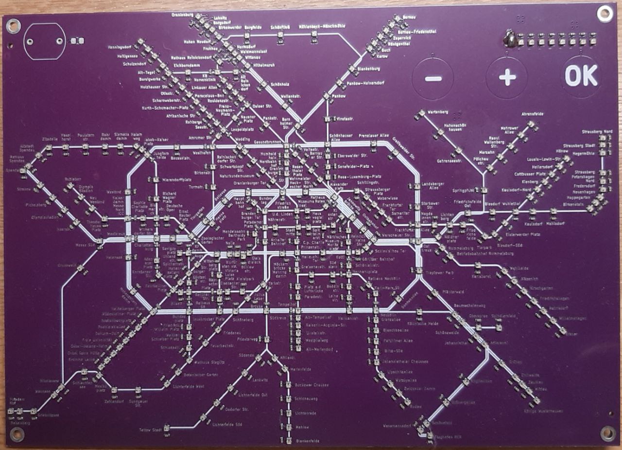
The manufactured board shown in the photos is V1 hardware. The design files in hw/ are a newer revision to work with the ESP32-S3 DevKitC-1 N16R8.
Scaling of the PCB can be done with a Python script. It includes automatic placement of the LEDs and routing in between. The scaled version only needs adjustment of the text size and placement of the ESP32 dev module connector.
The current software lives in sw/. It is developed using VS Code, PlatformIO, and ESP-IDF and currently targets the esp32-s3-devkitc-1-n16r8.
Build from the repository root:
cd sw
pio run -e esp32-s3-devkitc-1-n16r8
It uses the REST API from derhuerst https://github.com/derhuerst/bvg-rest to get information about active rides on a certain suburban or subway line and displays the station where the train arrives next.
sw/secrets.example.env to sw/secrets.env; the file is ignored by git and is used by the build and upload helpers.sw/tools/generate_ota_secrets.sh generates the ignored firmware header from sw/secTARGET_GIT_REPO_DIR=/path/to/fw_ota.rets.env. sw/upload.sh runs this automatically before building.sw/upload.sh is a local release helper. It increments sw/version.txt, builds firmware.bin, copies it into a separate OTA Git repository, commits it there, and pushes that OTA repository. Put TARGET_GIT_REPO_DIR in sw/secrets.env or pass the OTA repo path as the first argument. If HTTPS push needs a token, set UPLOAD_GIT_TOKEN there too.The PCB has been designed to be minimal in size to reduce manufacturing cost. It can be scaled using the KiCad IPC API. This requires KiCad 9 and above. The IPC API has some quirks. Most important, it needs to be enabled in the KiCad settings.
The photos currently show only the manufactured V1 hardware. The current KiCad revision is untested.
 V1 manufactured board
| Qty | Value | Footprint | References |
|---|---|---|---|
| 320 | XL-1010RGBC-WS2812B | SK6805-EC10-000:SMD-4P,1.1x1.1mm | U1, U10, U11, U100, U101, U102, U103, U104, U105, U106, U107, U108, U109, U110, U111, U112 +304 |
| 4 | MountingHole | MountingHole:MountingHole_2.2mm_M2_DIN965_Pad | H1, H2, H3, H4 |
| 3 | ~ | ESP32_DEVKITC_32UE:cap_touch | U322, U323, U324 |
| 1 | 74HC14 | Package_SO:SOIC-14_3.9x8.7mm_P1.27mm | U327 |
| 1 | C | Capacitor_SMD:CP_Elec_8x10 | C321 |
| 1 | ESP32-DEVKITC-32UE | ESP32_DEVKITC_32UE:ESPRESSIF_ESP32-DEVKITC-32UE | U321 |
| 1 | R | Resistor_SMD:R_0805_2012Metric_Pad1.20x1.40mm_HandSolder | R1 |
| 1 | SYM_EasterEgg_42x60mm | bb:Logo_Elektrojupp | SYM1 |

nichtrami/led_tube
A LED Tube that works wireless and runs on a ESP32 with Arduino Framework

Romemu1810-tech/bluetooth_jammer_experimento
Proyecto personal y experimental para el aprendizaje de electrónica, RF y comunicaciones Bluetooth, desarrollado con fines educativos y de investigación.

14chanwa/MiAM_robotics_ESP32
MiAM robotics repository for ESP32 based PAMIs and boards

adli-syauqi/general-purpose-mobile-robot-pcb
KiCad hardware design for a custom ESP32 general-purpose mobile robot controller. This board was made to drive 4-wheel omni and mecanum transporter robots.

arsya-stary/project-TARS
ini adalah project individual saya dan team saya untuk membuat robot TARS yang berada di dalam film INTERSTELLAR


It measures 153 × 107 mm and has 2 copper layers, 1.6 mm thick.
332 parts, built around the ESP32-DEVKITC-32UE, XL-1010RGBC-WS2812B-DZ and 74HC14. The full list of its parts is on this page, with links to each part's symbol and footprint where PCBKit's library has them.
From the elektrojupp/berlin_bahn repository on GitHub, at the commit this page was made from: the board is hw/berlin_bahn.kicad_pcb and its schematic hw/20xLED_001.kicad_sch. PCBKit opens the board in the browser, with nothing to install.
Its repository publishes it under the Apache-2.0 licence: you may reuse it on that licence's terms (keep the author's notice, and for a copyleft licence share your changes alike).