

4 layers177 × 110 mm

 dylanmsu/Ultrasonic_Phased_Array22
This repository contains all the sources for a working ultrasonic phased array powered by a ZYNQ FPGA.
PhasedArray is an open-source printed circuit board by dylanmsu, from the dylanmsu/Ultrasonic_Phased_Array repository on GitHub, published under the GPL-2.0 licence. It is a 4-layer board of 50 × 75 mm with 132 parts on 171 nets, routed with 954 tracks and 247 vias.
It is built around the TC4428AEOA and 74AHCT595D. Its parts include 59 capacitors, 30 ICs, 16 resistors and 2 connectors. It belongs with the fPGA and programmable logic boards of this library.
This repository is under construction and will contain all the sources for a working ultrasonic phased array. The vitis project in this repository is to be used in a accoustic levitation example.
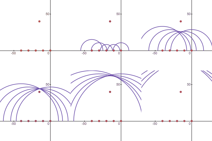
Lets consider an example where we want to send a single pulse of airpressure to a certain point in space. We have an array of transducers we can work with. Since the waves travel in a sphere around the transducers, we can time the pulses at each transducer in such a way that all the wavefronts arrive at the same time in a single focal point. This is illustrated in the animation below.
 [blocked]
If we were to send a sinewave with the same delay through the transducers instead of a single pulse, all the peaks and troughs of those waves would ideally only add up in the focal point. The amplitude would then be the greatest at that point and ideally cancel out everywhere else. This is actually not always the case because a side effect of using a periodic signal is that we create te posibility of sidelobes. Sidelobes are areas where some of the sinewaves constructively add up unwantedly where the phase shift is a multiple of 360 degrees. To prevent the occurance of sidelobes, we need to space the transducers with a distance between 1/2 wavelength, and 1/4 wavelength.
To calculate the phase offsets per transducer for a single focal point, the following formula is used: $$\varphi = -\frac{2\pi\sqrt{(X_t - X_f)^2 + (Y_t - Y_f)^2 + (Z_t - Z_f)^2}}{\lambda}$$ Where:
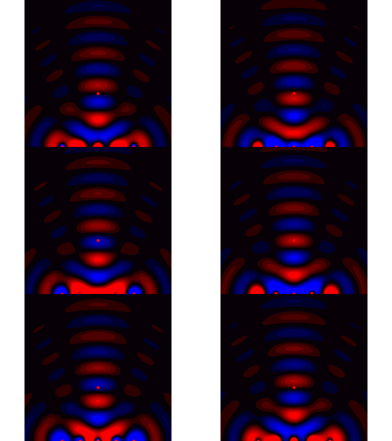
The waves exiting the transducers will look something like this.
 [blocked]
The red dots at the bottom are sources emitting pure sinusodial signals with an adjusted phase delay so all the waves are in phase at the red dot around the middle.
There is an included python script called 'wave_equation.py' that focuses the waves to your mouse location by manipulating the phases of the emitters. It solves the 2d wave equation so it should be more acurate than the above animation.
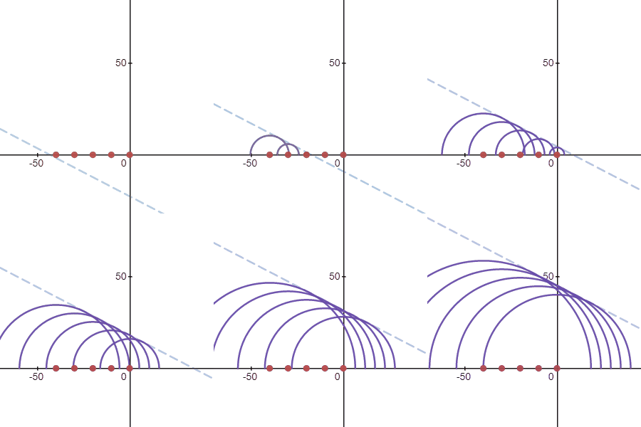
We can also steer a beam into a specified direction. To do this we have to align the wavefronts into a plane where its normal vector points to the direction of travel. This is illustrated in 2d in the animation below.
 [blocked]
Here the phase offsets are calculated using the following formula: $$\varphi = \frac{2\pi(aX_t+bY_t-Z_t)}{\lambda\sqrt{1+a^2+b^2}}$$ Where:
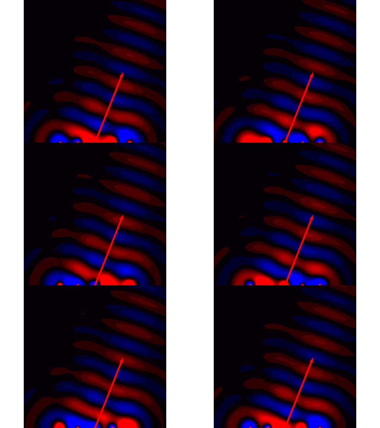
The waves exiting the transducers will look something like this.
 [blocked]
In the case for this project, the spacing between the sources is 10 mm wich is more than double the recommended wavelength so we expect some loss of energy through sidelobes. Even more so diagonally since the sources are placed in a rectangular grid and the diagonal spacing is 14.14 mm. Placing the sources in a hexagonal grid solves big diagonal spacing but this makes the design of the PCB more challanging. For this reason i opted to design a rectangular grid of sources anyway.
There are two array's used in the levitation example. One is facing upwards and the other is facing downwards. They are facing eachother with a distance of 70mm. This distance is arbitrarily chosen based on the needed volume for levitation.
The FPGA used in this project is the ZYNQ XC7Z020 on a Zybo Z7 board but any Zynq FPGA should work. The FPGA contains two distinct parts: The processing system (PS) and the programmable logic (PL):
The PL contains an implementation which receives 7 bit values from the PS (Processing System) for every transducer. This value sets the phase of the output signal. This is acheived by making a fifo of length = 2^7 in the case of a phase resolution of 7 bits. The 40KHz signal is fed into the fifo at 40KHz * 2^7 = 5.12MHz. The reason for this is because we want exactly 1 full period of the signal in the fifo. The 7 bit value determines at which address of the fifo the output signal is tapped from. This way wan can adjust the phase of the output signal in 2^7 steps per period.
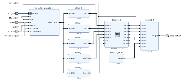
The block diagram that takes an AXI peripheral bus and outputs a serial data stream to drive the included transducer board is illustrated below.
 [blocked]
here is an overview of the in- and output signals:
The AXI peripheral IP_block generates the delayed signals and outputs them as a 25 bit vector. This vector is split into 5x 5 bit vectors by the xlslice blocks. The 5 bit vectors enter the seializer. The data is then clocked bit by bit to the output.
 [blocked]
TODO
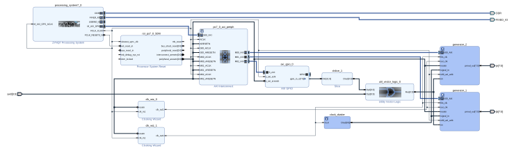
The Processing system sends data to the FPGA facric which adjusts the phase offsets of the physical transducers.
In an ideal world the signal applied to the physical transducer should give the same signal in air pressure. That is however not the case. For every transducer there is a significant random phase shift present. This will completely negate our effort to acheive a phased array. So we have to measure the phase shift of every transducer and incorporate this into the phase calculations.
Below is a video showing two ultrasonic arrays levitating a piece of styrofoam in an preprogrammed path.

| Qty | Value | Footprint | References |
|---|---|---|---|
| 30 | 100nF | Capacitor_SMD:C_0603_1608Metric | C11, C13, C15, C17, C19, C21, C23, C25, C27, C29, C31, C33, C35, C37, C39, C41 +14 |
| 28 | 4.7uF | Capacitor_SMD:C_0805_2012Metric | C1, C2, C3, C10, C12, C14, C16, C18, C20, C22, C24, C26, C28, C30, C32, C34 +12 |
| 25 | Speaker_Ultrasound | MA40S4R:XDCR_MA40S4R | LS1, LS2, LS10, LS11, LS12, LS13, LS14, LS15, LS16, LS17, LS18, LS19, LS20, LS21, LS22, LS23 +9 |
| 25 | TC4428AEOA | TC4428AEOA:SOIC127P600X175-8N | U1, U2, U10, U11, U12, U13, U14, U15, U16, U17, U18, U19, U20, U21, U22, U23 +9 |
| 15 | 39R | Resistor_SMD:R_0402_1005Metric | R2, R3, R4, R5, R6, R7, R8, R9, R10, R11, R12, R13, R14, R15, R16 |
| 5 | 74AHCT595 | Package_SO:TSSOP-16_4.4x5mm_P0.65mm | U26, U27, U28, U29, U30 |
| 1 | 0R | Resistor_SMD:R_0603_1608Metric_Pad0.98x0.95mm_HandSolder | R1 |
| 1 | 47uF | Capacitor_SMD:C_Elec_5x5.4 | C59 |
| 1 | Conn_02x06_Odd_Even | Connector_PinHeader_2.54mm:PinHeader_2x06_P2.54mm_Horizontal | J2 |
| 1 | Screw_Terminal_01x02 | TerminalBlock_Phoenix:TerminalBlock_Phoenix_PT-1,5-2-3.5-H_1x02_P3.50mm_Horizontal | J3 |
It measures 50 × 75 mm and has 4 copper layers, 1.6 mm thick.
132 parts, built around the TC4428AEOA and 74AHCT595D. The full list of its parts is on this page, with links to each part's symbol and footprint where PCBKit's library has them.
From the dylanmsu/Ultrasonic_Phased_Array repository on GitHub, at the commit this page was made from: the board is hardware/PhasedArray5x5/PhasedArray.kicad_pcb and its schematic hardware/PhasedArray5x5/PhasedArray.kicad_sch. PCBKit opens the board in the browser, with nothing to install.
Its repository publishes it under the GPL-2.0 licence: you may reuse it on that licence's terms (keep the author's notice, and for a copyleft licence share your changes alike).

Amir-imani/Autonomous-Mobile-Robot
Thesis project: Design and Construction of a Mobile Robot with Intelligent Path Planning in Dynamic Environments.


dan-rodrigues/ym2610-pcb
FPGA-based PCB to control a YM2610 sound synthesis chip.

MitchBradley/Esp32PrinterController
PCB design for 3D printer controller using ESP32 processor


maddoxlab/spdif-splitter
Design files and code for S/Plitter, a box that turns optical S/PDIF signals into separate TTL bits for EEG triggering in auditory experiments
