

4 layers99 × 53.3 mm
PSLab
fossasia/pslab-hardware
PSLab Hardware Design and Schematics https://pslab.io
199 parts1.7kApache-2.0

Just another keyboard
Jak is an open-source printed circuit board by drewlwhitney, from the drewlwhitney/jak repository on GitHub. It is a 2-layer board of 230.3 × 96.9 mm with 93 parts on 80 nets, routed with 442 tracks and 64 vias.
It is built around the 1N4148W. Its parts include 36 diodes and 36 switches. It belongs with the nRF52 and nRF5x boards of this library.
The PCB is non-reversible and is designed for Gateron KS-33 Low Profile Switches with hotswap sockets.
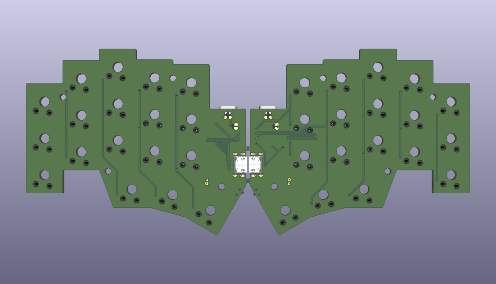 Front
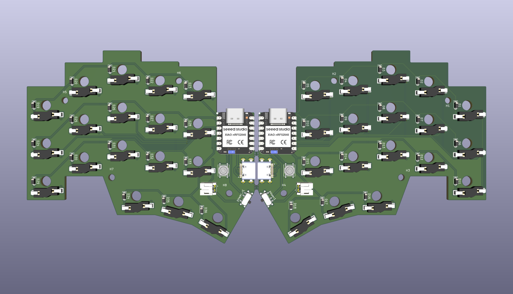 Back
This was written on January 7, 2026 for JLCPCB.
Upload the PCB Gerber Files (.zip) to JLCPCB, then leave everything as-is except for:
| Option | Value |
|---|---|
| Different Design | 2 |
| PCB Color | Your choice |
| Qty | Value | Footprint | References |
|---|---|---|---|
| 36 | 1N4148W | Diode_SMD:D_SOD-123 | D1, D2, D10, D11, D12, D13, D14, D15, D16, D17, D18, D19, D20, D21, D22, D23 +20 |
| 36 | SW_Push | Gateron_KS33_Hotswap:Gateron-KS33-Hotswap-1U | SW1, SW10, SW10_r1, SW11, SW11_r1, SW12, SW12_r1, SW13, SW13_r1, SW14, SW14_r1, SW15, SW15_r1, SW16, SW16_r1, SW17 +20 |
| 8 | MountingHole | MountingHole:MountingHole_3.2mm_M3 | H1, H2, H3, H4, H5, H6, H7, H8 |
| 2 | PTS526 SM15 SMTR2 LFS | footprints:SON4_PTS526 SM15 SMTR2 LFS_CNK | RES_r1, RES1 |
| 2 | SW_SPDT | Button_Switch_SMD:SW_SPDT_PCM12 | power_r1, power1 |
| 2 | USB_C_Receptacle_USB2.0_14P | USB4505-03-0-A_REVA:GCT_USB4505-03-0-A_REVA | split_connector_r1, split_connector1 |
| 2 | XIAO-nRF52840-SMD | jak:XIAO-nRF52840-SMD-underside | controller_r1, controller1 |
| 1 | Conn_01x02 | S2B-PH-K-S_LF__SN_:JST_S2B-PH-K-S_LF__SN_ | jst1 |
| 1 | S2B-PH-K-S_LF__SN_ | S2B-PH-K-S_LF__SN_:JST_S2B-PH-K-S_LF__SN_ | jst_r1 |
The 90 most common of 93 parts.
It measures 230.3 × 96.9 mm and has 2 copper layers, 1.6 mm thick.
93 parts, built around the 1N4148W. The full list of its parts is on this page, with links to each part's symbol and footprint where PCBKit's library has them.
From the drewlwhitney/jak repository on GitHub, at the commit this page was made from: the board is pcb/jak.kicad_pcb and its schematic pcb/jak.kicad_sch. PCBKit opens the board in the browser, with nothing to install.
Its repository states no licence, so its author keeps all rights: ask drewlwhitney before reusing the design.
fossasia/pslab-hardware
PSLab Hardware Design and Schematics https://pslab.io

pierrechevalier83/ferris
A low profile split keyboard designed to satisfy one single use case elegantly


MickiusMousius/Rolio46Keyboard
A split wireless keyboard based on the Corne and Sofle


sadekbaroudi/bgkeeb
This is a reversible 100mm x 100mm pcb with support for mx or choc switches (no hotswap), per key led, rotary encoders, and exposes the SDA/SCL/GND/VCC lines in the form of the pimoroni trackball pins (meaning you can…
