2 layers
Amplificador
nachocarballeda/gclass_amplifier
Diseño de un amplificador clase G para la materia Circuitos Electronicos 2. FIUBA
92 parts3
 dmsherazi/Battery-Management-System1
Solar-battery charge regulator
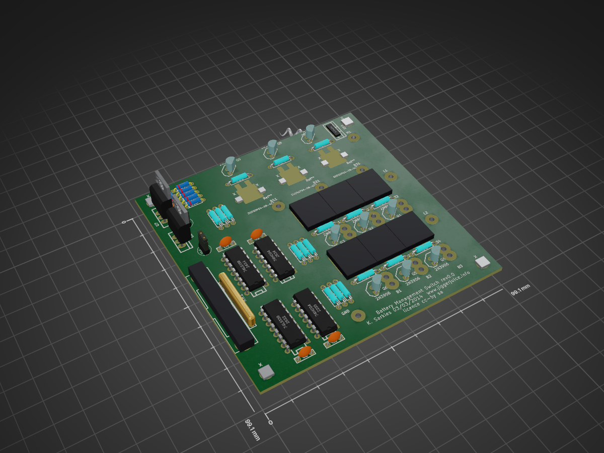
Switch electronics is an open-source printed circuit board by dmsherazi, from the dmsherazi/Battery-Management-System repository on GitHub, published under the GPL-3.0 licence. It is a 2-layer board of 99.1 × 99.1 mm with 95 parts on 81 nets, routed with 548 tracks and 3 vias.
It is built around the 74HC04D, 74LS139PC and LM1084IT-3.3/NOPB, with the LM7809CT, SQD45P03-12-GE3-VB and SUD50P04-08-GE3 among its other parts. Its parts include 18 resistors, 15 transistors, 7 capacitors, 7 diodes and 6 ICs. It belongs with the power boards of this library.


PCB for the MOSFET switch matrix.
Digital circuitry ensures that no two batteries are connected together, which could cause damage if the state of charge differs significantly.
A diode matrix is used to provide power for the electronics. It ensures that power is taken from the loads, or from the batteries if the loads are not connected. This enables the firmware to keep track of the current drawn by the local electronics.
The MOSFETs are driven by simple BJT-resistor drivers. This results in quite slow switching speeds. There may be a need for faster switching e.g. high speed PWM to reduce EMI. In this case the circuit needs to be modified to use better drivers.
There were several errors in the circuit, which have been corrected but not tested. The board is to be replaced with the gEDA version.
In the board, load 1 is the central row of switches and the upper power connector. Load 2 is the lower row of switches and the lower power connector. This is the reverse of that used in the interconnect board and has been changed in the gEDA board.
(c) K. Sarkies 26/04/2014
| Qty | Value | Footprint | References |
|---|---|---|---|
| 19 | CONN_1 | SolderWirePad_single_2mmDrill | B1, B2, B3, B11, B12, B13, B14, B21, B22, B23, B24, B31, B32, B33, B34, GND +3 |
| 14 | SolderWirePad_single_1mmDrill | SolderWirePad_single_1mmDrill | X, X, X, X, X, X, X, X, X, X, X, X, X, X |
| 9 | 10K | R4 | R1, R2, R3, R4, R5, R6, R7, R8, R9 |
| 9 | 1K | R4 | R10, R11, R12, R13, R14, R15, R16, R17, R18 |
| 9 | 2N3906 | TO92-CBE | Q1, Q2, Q3, Q4, Q5, Q6, Q7, Q8, Q9 |
| 6 | SQD45P03-12-GE3 | TO252-HS-S | Q10, Q12, Q13, Q15, Q16, Q18 |
| 5 | 0.1uF | C2 | C1, C2, C3, C4, C8 |
| 4 | 1N4701 | D3 | D7, D8, D9, D11 |
| 4 | SolderWirePad_single_2mmDrill | SolderWirePad_single_2mmDrill | X, X, X, X |
| 3 | SUD50P04-08-GE3 | Fred:TO252-HS | Ref**, Ref**, Ref** |
| 2 | 10uF | C1V5 | C9, C10 |
| 2 | 1N5819 | D3 | D12, D13 |
| 2 | 74HC04 | DIP-14__300 | U1, U3 |
| 2 | 74LS139 | DIP-16__300 | U2, U4 |
| 1 | 10K | r_pack8 | RR1 |
| 1 | CONN_12 | he10-14d | P1 |
| 1 | LM1084IT-3.3/NOPB | Transistors_TO-220:TO-220_Neutral123_Vertical | U8 |
| 1 | LM7809CT | TO-220_Neutral123_Vertical | U7 |
| 1 | MBR1645 | Diode_TO-220_Vertical | D10 |
nachocarballeda/gclass_amplifier
Diseño de un amplificador clase G para la materia Circuitos Electronicos 2. FIUBA

Boardoza/Boardoza_VNH7070AS_Bidirectional_DC_Motor_Driver_Breakout_Board
Compact VNH7070AS-based full-bridge motor driver breakout board for bidirectional DC motor control with PWM and current sensing.


It measures 99.1 × 99.1 mm and has 2 copper layers, 1.6 mm thick.
95 parts, built around the 74HC04D, 74LS139PC, LM1084IT-3.3/NOPB and LM7809CT. The full list of its parts is on this page, with links to each part's symbol and footprint where PCBKit's library has them.
From the dmsherazi/Battery-Management-System repository on GitHub, at the commit this page was made from: the board is Kicad-Switch/switch-electronics.kicad_pcb. PCBKit opens the board in the browser, with nothing to install.
Its repository publishes it under the GPL-3.0 licence: you may reuse it on that licence's terms (keep the author's notice, and for a copyleft licence share your changes alike).