
4 layers234 × 84 mm
Main panel
google/mozc-devices
Circuit diagrams and firmware source code for Gboard DIY keyboards
234 parts3kApache-2.0

 dhyans26/BluPad1
BOM (There honestly might be more stuff, I made this a while back- will update when my macropad comes in) --- 1. 9 Cherry MX Switches 2. Rotary Switch Encoder 3. Keycaps! 4. Xiao Seeed rp2040
HackPad is an open-source printed circuit board by dhyans26, from the dhyans26/BluPad repository on GitHub, published under the MIT licence. It is a 2-layer board of 82 × 95.5 mm with 31 parts on 31 nets, routed with 247 tracks and 21 vias.
It is built around the SK6812MINI-E. Its parts include 17 diodes, 10 switches and 1 IC. It belongs with the RP2040 boards of this library.

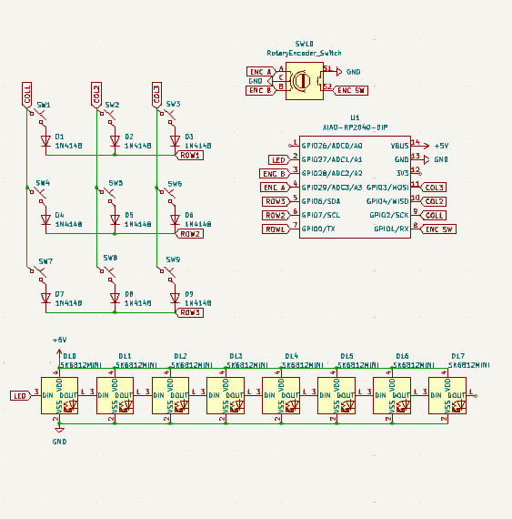


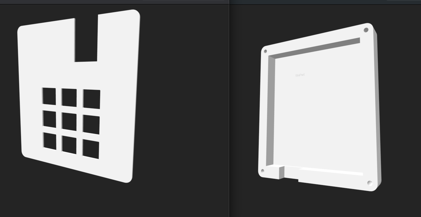
This was unlike anything I have undertaken before and I do not know if my HackPad has all the necessary components. I had many challenges that I had to persevere through while attempting to make my own macropad. At this point in time while it very possibly does not work in it's current form but I am proud of what I have accomplished so far. The first hurdle occured in KiCad where no matter how many times I imported the OPL + SEEED libraries I never got the same footprint as the tutorials so I had to figure out how to use a similar one. Then in KiCad the right menu bar dissapeared (idk why / how) and I couldn't find anywhere online how to make it appear. The elements on the PCB editor was barely visable and I finally got help in the Slack today on how to fix it (this set me back multiple days). The libraries still didn't import the 3d render of the Xiao in the viewer but I think I can solder it on. Routing the copper wires from the ratsnest and organizing the layout was pretty fun :) ! Fusion was unfortunately very slow and took roughly an hour just to get downloaded and setup on my laptop (Fusion is just slow- I didn't do anything) Even through this all, for my first attempt at ever designing a PCB I do not think I did too bad. This has got me interested in hardware based projects and I am definitely planning on persuing deeper into the field!
| Qty | Value | Footprint | References |
|---|---|---|---|
| 9 | 1N4148 | Diode_THT:D_DO-35_SOD27_P7.62mm_Horizontal | D1, D2, D3, D4, D5, D6, D7, D8, D9 |
| 9 | SW_Push_45deg | Button_Switch_Keyboard:SW_Cherry_MX_1.00u_PCB | SW1, SW2, SW3, SW4, SW5, SW6, SW7, SW8, SW9 |
| 8 | SK6812MINI | LED_SMD:LED_SK6812MINI_PLCC4_3.5x3.5mm_P1.75mm | D10, D11, D12, D13, D14, D15, D16, D17 |
| 3 | LOGO | LOGO | G***, G***, G*** |
| 1 | RotaryEncoder_Switch | Rotary_Encoder:RotaryEncoder_Alps_EC11E-Switch_Vertical_H20mm | SW10 |
| 1 | XIAO-RP2040-DIP | OPL:XIAO-RP2040-DIP | U1 |
It measures 82 × 95.5 mm and has 2 copper layers, 1.6 mm thick.
31 parts, built around the SK6812MINI-E. The full list of its parts is on this page, with links to each part's symbol and footprint where PCBKit's library has them.
From the dhyans26/BluPad repository on GitHub, at the commit this page was made from: the board is PCB/HackPad.kicad_pcb and its schematic PCB/HackPad.kicad_sch. PCBKit opens the board in the browser, with nothing to install.
Its repository publishes it under the MIT licence: you may reuse it on that licence's terms (keep the author's notice, and for a copyleft licence share your changes alike).
google/mozc-devices
Circuit diagrams and firmware source code for Gboard DIY keyboards

Bastardkb/Dilemma
The Dilemma is a vertical stagger low-profile keyboard with mods.

Pwnsat/FlatSat
Flatsat v1.0 is a hardware based platform for aerospace cybersecurity research

adamws/kicad-kbplacer
KiCad plugin for automatic keyboard's key placement and routing

imchipwood/dumbpad
Simple 4x4 numpad with rotary encoder. Powered by QMK via ATmega32u4 Pro Micro

makerforgetech/modular-biped
An open source framework for creating a bipedal modular companion robot.

