


2 layers77.5 × 100 mm
Rover pdb
devkyber/PCB
AI-assisted PCB engineering for native KiCad: source evidence, scoped changes, checked previews, human review, and reproducible release packages.
93 parts
 devkyber/PCB
AI-assisted PCB engineering for native KiCad: source evidence, scoped changes, checked previews, human review, and reproducible release packages.
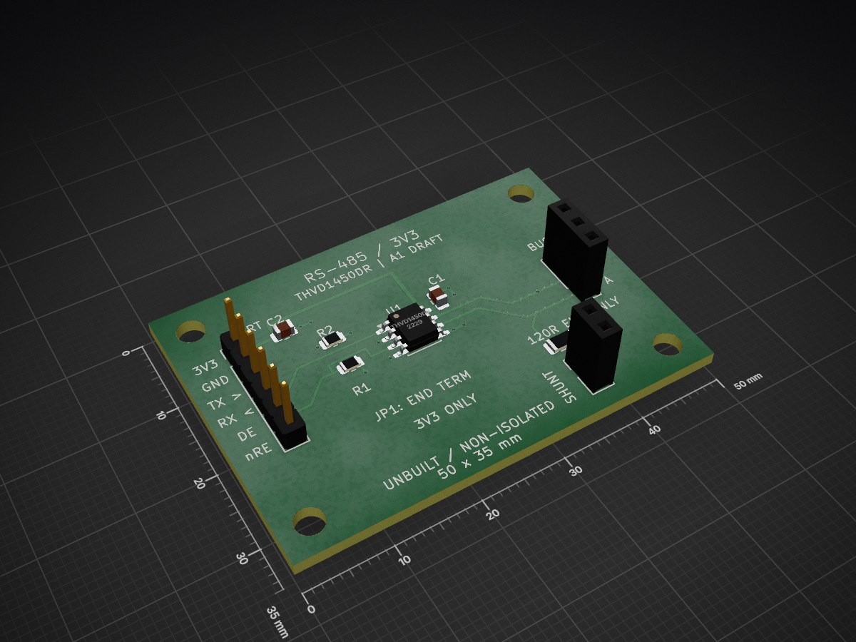
Rs485-interface is an open-source printed circuit board by devkyber, from the devkyber/PCB repository on GitHub. It is a 2-layer board of 50 × 35 mm with 13 parts on 9 nets, routed with 52 tracks and 12 vias.
It is built around the THVD1450DRBR, CRCW080510K0FKEAC and CC0805KKX7R7BB105, with the CC0805KRX7R9BB104, CRCW1206120RFKEAC and HTSW-103-07-G-S among its other parts. Its parts include 3 resistors, 2 capacitors, 2 connectors and 1 IC. It belongs with the interfaces and adapters boards of this library.


An unbuilt educational DRAFT for trying PCB Copilot on a complete, small KiCad design. Four independent 0 to 3.3 V inputs drive four red LEDs through 1.1 kOhm resistors. The 45 x 35 mm board has two copper layers, through-hole components, two mounting holes, project-local libraries and all three package models.
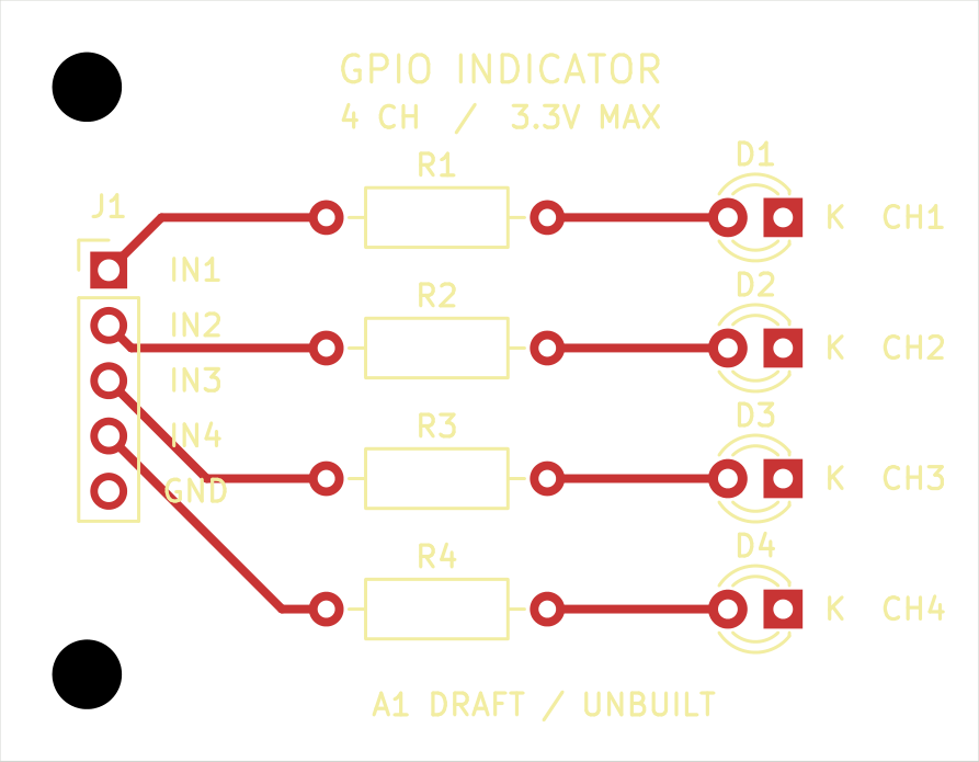
Open gpio-indicator.kicad_pro in KiCad 10, or inspect the schematic PDF, schematic image, assembly drawing, front copper and mirrored underside. The GLB model is a native CAD visualization; it does not establish actual component fit.
From the repository root:
uv run pcb-copilot doctor
uv run pcb-copilot status examples/gpio-indicator
uv run pcb-copilot research examples/gpio-indicator --verify
uv run pcb-copilot research examples/gpio-indicator --verify-schematic-parts
uv run pcb-copilot review examples/gpio-indicator
The last command deliberately returns exit 1: supplier assembly rotation contracts and all five human review decisions are absent. Native ERC and DRC are clean, connectivity and forward-annotation links agree, and the independent dated JLCPCB geometry check passes. These results are scoped machine checks, not fabrication approval or measured performance. See the saved review and author inspection record.
J1 pins 1 through 4 are IN1 through IN4; pin 5 is GND. It has no power pin. With a 3.3 V input and initial 1% resistance tolerance, the calculation gives at most 3.031 mA per channel, taking no credit for LED forward voltage. That loading must suit the actual controller's per-pin and aggregate drive limits. Actual brightness, current, fit, assembly and external-controller behavior remain unqualified.
The resistor was deliberately chosen as 1.1 kOhm: 1 kOhm at its negative 1% tolerance would allow a 3.333 mA zero-Vf bound. The requirements and design basis state the assumptions and scope. This example has no ESD protection, isolation, level conversion, voltage regulation or approval for an application.
Exact manufacturer PDF bytes are in evidence. The library receipt binds official KiCad footprint copies, pad functions, manufacturer evidence and local model bytes to their hashes. The local footprint files change only model URIs. Board instances use wider silkscreen strokes to meet the workspace baseline; numbered pad geometry is unchanged. Generic package models are visualization aids.
The saved native CAD is authoritative. A construction script must not overwrite later edits. Use a separate copy for experiments and the shared candidate workflow for checked updates. No owner board or frozen test fixture was modified to create this example.
| Qty | Value | Footprint | References |
|---|---|---|---|
| 4 | M3 NPTH | RS485:MountingHole_3.2mm_M3 | H1, H2, H3, H4 |
| 2 | 10 kOhm | RS485:R0805_10k | R1, R2 |
| 1 | 1 uF | RS485:C0805_1uF | C2 |
| 1 | 100 nF | RS485:C0805_100nF | C1 |
| 1 | 120 Ohm | RS485:R1206_120R | R3 |
| 1 | BUS / A B GND | RS485:BUS_HTSW103 | J2 |
| 1 | HTSW-102-07-G-S | RS485:TERM_HTSW102 | JP1 |
| 1 | THVD1450DR | RS485:SOIC8_THVD1450DR | U1 |
| 1 | UART / 3V3 | RS485:UART_HTSW106 | J1 |
It measures 50 × 35 mm and has 2 copper layers, 1.6 mm thick.
13 parts, built around the THVD1450DRBR, CRCW080510K0FKEAC, CC0805KKX7R7BB105 and CC0805KRX7R9BB104. The full list of its parts is on this page, with links to each part's symbol and footprint where PCBKit's library has them.
From the devkyber/PCB repository on GitHub, at the commit this page was made from: the board is examples/rs485-interface/rs485-interface.kicad_pcb and its schematic examples/gpio-indicator/gpio-indicator.kicad_sch. PCBKit opens the board in the browser, with nothing to install.
Its repository states no licence, so its author keeps all rights: ask devkyber before reusing the design.
devkyber/PCB
AI-assisted PCB engineering for native KiCad: source evidence, scoped changes, checked previews, human review, and reproducible release packages.

devkyber/PCB
AI-assisted PCB engineering for native KiCad: source evidence, scoped changes, checked previews, human review, and reproducible release packages.

devkyber/PCB
AI-assisted PCB engineering for native KiCad: source evidence, scoped changes, checked previews, human review, and reproducible release packages.

devkyber/PCB
AI-assisted PCB engineering for native KiCad: source evidence, scoped changes, checked previews, human review, and reproducible release packages.

NOAA-PMEL/ASVCO2
Open Source Repository for the Autonomous Surface Vehicle CO2 (ASVCO2) gen2 system

mcapdeville/esp32s3aprs
ESP32s3 APRS beacon/tracker/logger, USB kiss TNC , USB audio FM tranceiver with Micropython shell

MixedSignalDevelopment/K2601-Doomsday-Comms-System
Editable source design for the Doomsday Comms System (D.C.S., SKU OS2601), board rev B.

PhysicsUofRAUI/hooting_owl
Hold code and eventually the pcb layout for my hooting owl retrofit

VikingMotorsports/Battery-Management-System-Capstone-2026
The BMS Capstones deliverables

cminyard/PacSatBaseBoard
Base board outline and connectors for PacSat boards


jodhsinghnahal/piezo_matlab
Simulation, circuit and PCB design repository for investigating piezoelectric energy harvesting (PEH) interfaces under conventional vibration excitation and underwater acoustic excitation.