
2 layers79 × 30 mm
LIA
JGAguado/LIA
Low-power pet tracking platform built around Meshtastic and LoRa mesh networking
81 parts29

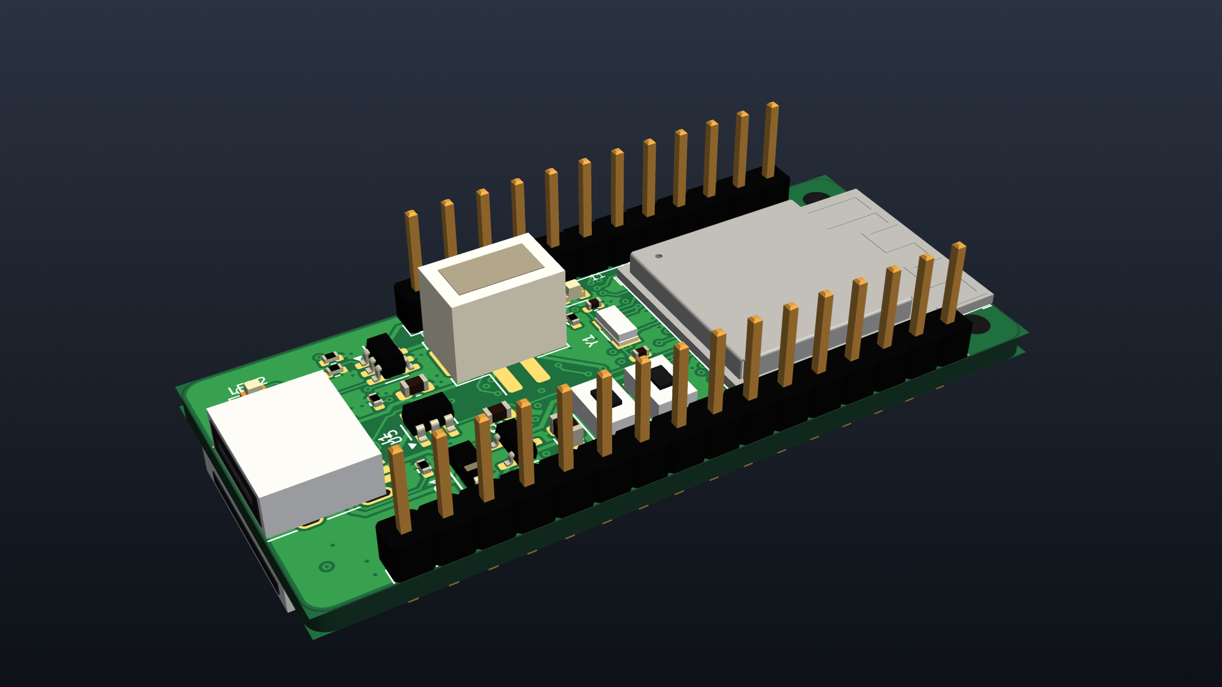
This folder holds the complete electronic CAD for the ZB-1 development board:
Zb1 is an open-source printed circuit board by danindiana, from the danindiana/zemizdat repository on GitHub, published under the Apache-2.0 licence. It is a 4-layer board of 50.8 × 22.9 mm with 71 parts on 57 nets, routed with 1,127 tracks and 149 vias.
It is built around the ESP32-S3-MINI-1-N8, DW01A and MAX17048G+T10, with the RT9080-33GJ5, USBLC6-2SC6 and B5819W among its other parts. Its parts include 25 resistors, 16 capacitors, 7 ICs, 6 connectors and 3 diodes. It belongs with the ESP32 boards of this library.


This folder holds the complete electronic CAD for the ZB-1 development board:
Everything is generated by scripts from one design database (scripts/zb1_design.py), so the
board can be rebuilt and every number below re-checked.
Licence:
- The ZB-1 hardware design is © 2026 Benjamin W. Denio under the CERN Open Hardware Licence v2 – Permissive.
- The generator scripts in
scripts/are under Apache-2.0.- The Espressif module footprint and STEP model keep their CC-BY-SA 4.0 licence (
lib/ATTRIBUTION.md).If you modify the design and share it, say so in your copy (CERN-OHL-P §3.3).
Status: design files, not a proven board. Nothing here has been fabricated, assembled or powered. The layout was placed by script and routed by an autorouter. DRC results are reported honestly in §5, including the items that still need a human. A qualified layout review is required before ordering boards; see the checklist in §7.
| Board | 50.8 × 22.86 mm (Adafruit Feather outline), 1.5 mm corner radius, 1.6 mm FR-4 |
| Layers | 4: F.Cu signal / In1 solid GND plane / In2 signal + GND fill / B.Cu signal + GND fill |
| Parts | 69 electrical parts + 2 mounting holes placed (7 of them DNP by default), top and bottom side |
| Routing | 1 127 track segments, 149 vias; 0.15 mm signal / 0.3 mm power / 0.2 mm USB tracks, 0.5/0.25 mm vias |
| Antenna | module antenna flush with the board edge; copper keep-out on all four layers past x = 45.4 mm |
| Netlist | schematic netlist checked pin by pin against the design database: OK — 69 components, 57 nets, 264 pin connections; the PCB pads were cross-checked the same way (0 mismatches) |
| DRC | 0 unconnected, 0 clearance / hole / short errors. 8 mechanical items waived (mounting-hole courtyards, edge-mount microSD shell), 94 cosmetic warnings (silkscreen, library-copy differences) — see §5 |
| Path | What it is |
|---|---|
zb1.kicad_pro, zb1.kicad_sch, zb1.kicad_pcb | KiCad 7 project: open zb1.kicad_pro in KiCad 7.0 or newer |
lib/zb1.kicad_sym | project symbols for parts KiCad 7 lacks: BQ21040, RT9080-33, DW01A, FS8205A, MAX17048 |
lib/zb1.pretty/ESP32-S3-MINI-1.kicad_mod | module footprint from espressif/kicad-libraries (CC-BY-SA 4.0 with the KiCad design exception) |
lib/3dmodels/ | Espressif module STEP model, plus simple dimensioned envelope bodies for parts without a KiCad 3D model (USB-C, microSD, both JST connectors, KMR2 switches, crystal) |
fab/zb1_gerbers.zip | Gerber X2 (11 layers) + Excellon drill (PTH and NPTH separate): upload this to a PCB fab |
fab/zb1_bom.csv | grouped BOM with MPNs; DNP lines marked |
fab/zb1_pos.csv | pick-and-place centroids, both sides, mm (DNP and through-hole parts excluded) |
docs/zb1_schematic.pdf | schematic, one A2 sheet in seven titled blocks |
docs/zb1_assembly_top.pdf, docs/zb1_assembly_bottom.pdf | assembly drawings (fab layer with every reference) |
docs/*drl_map.pdf | drill maps |
3d/zb1.step | whole assembly for enclosure/mechanical CAD (FreeCAD, Fusion, Onshape, SolidWorks) |
images/ | schematic PNG, per-copper-layer plots, board-surface images, 3D renders |
reports/drc.rpt | full KiCad DRC report |
reports/netlist_check.txt | schematic-vs-design-database check |
scripts/ | the generators (§6) |
build.sh | rebuilds everything above from scripts/zb1_design.py |
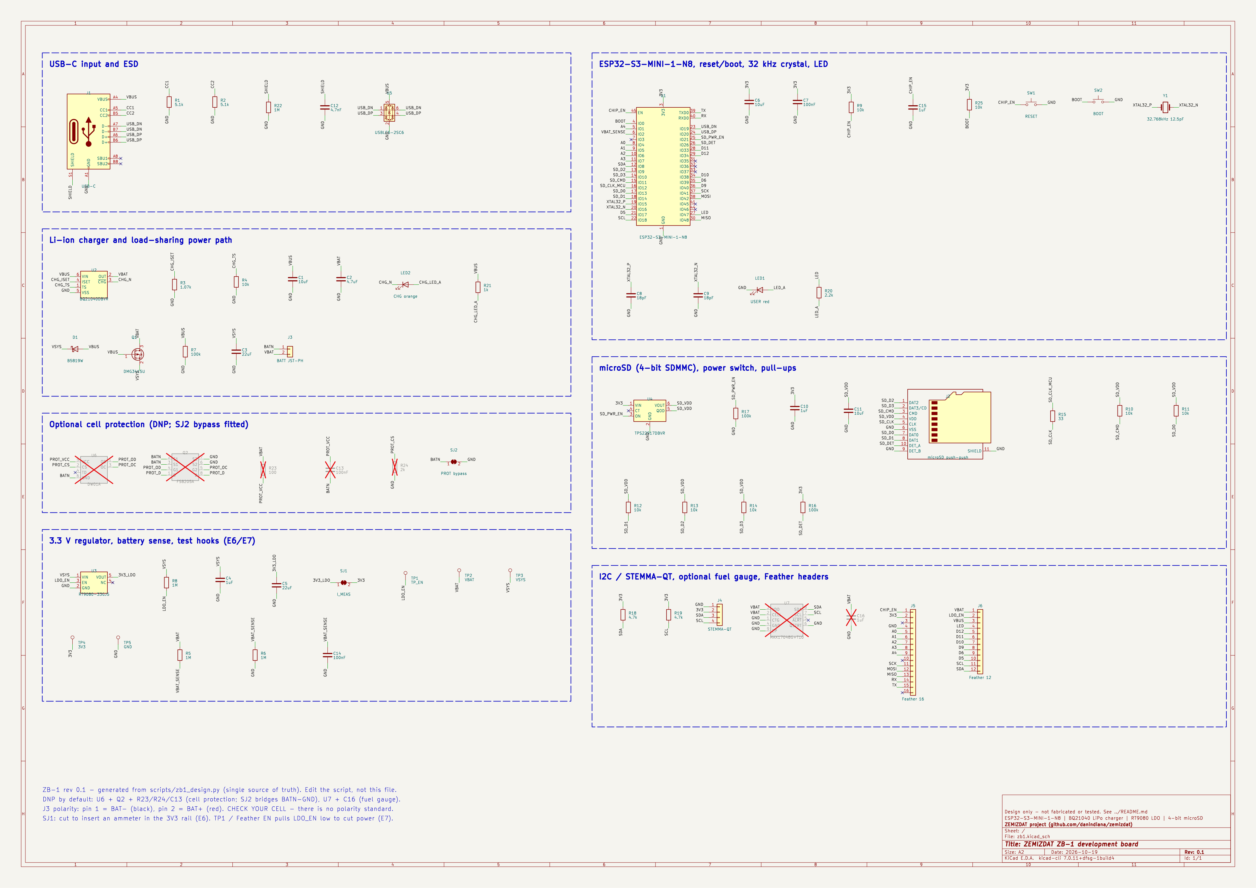
The schematic implements exactly the circuit in ../README.md §3–§5. It is drawn
in a "label per pin" style: every pin gets a short stub with its net label. It is generated from
zb1_design.py, so edit that file and regenerate rather than editing the schematic by hand.
reports/netlist_check.txt confirms that the netlist KiCad exports from the schematic matches the
database:
Changes from the earlier text description, made while drawing it:
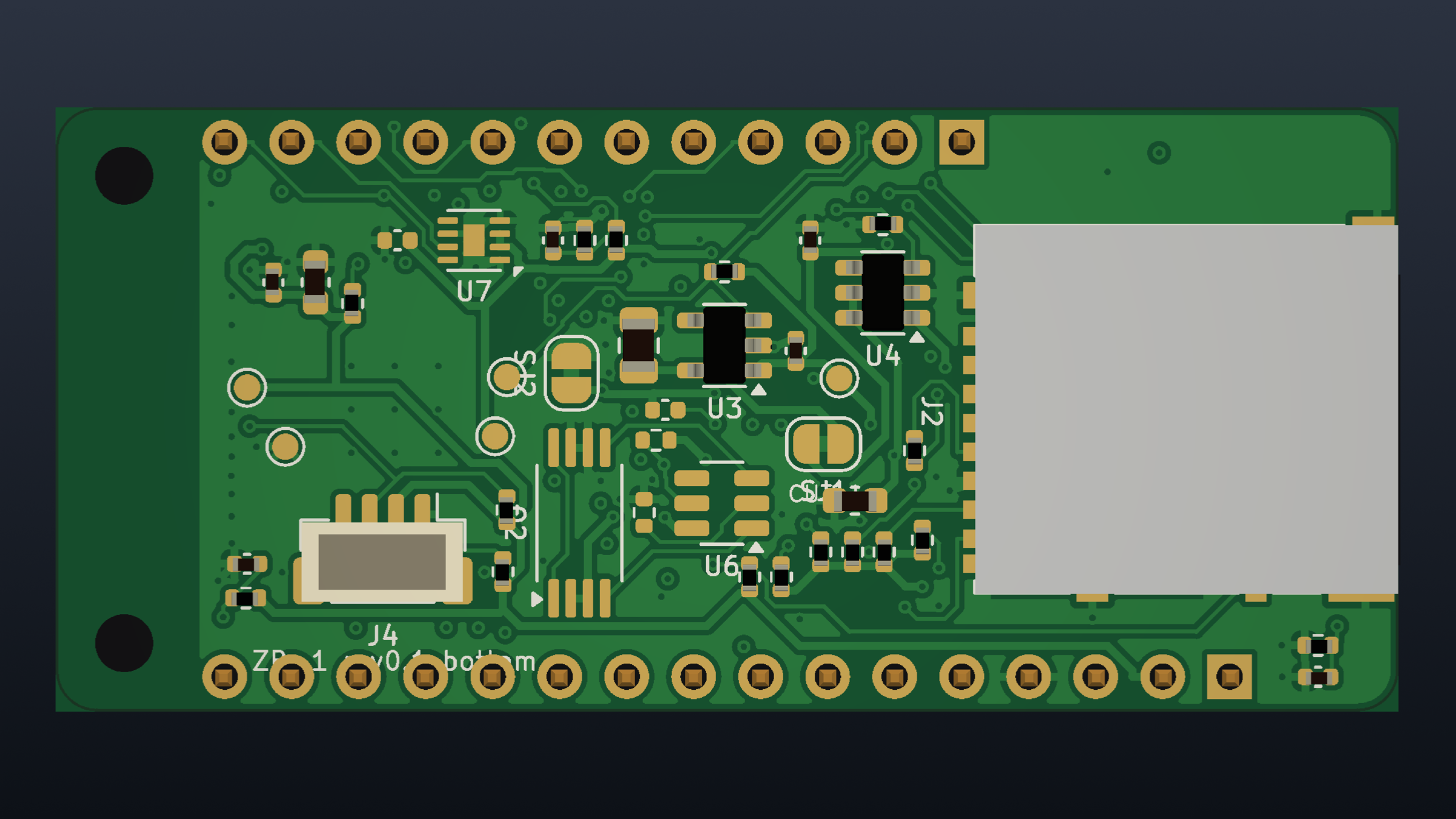
| Top | Bottom (seen from below) |
|---|---|
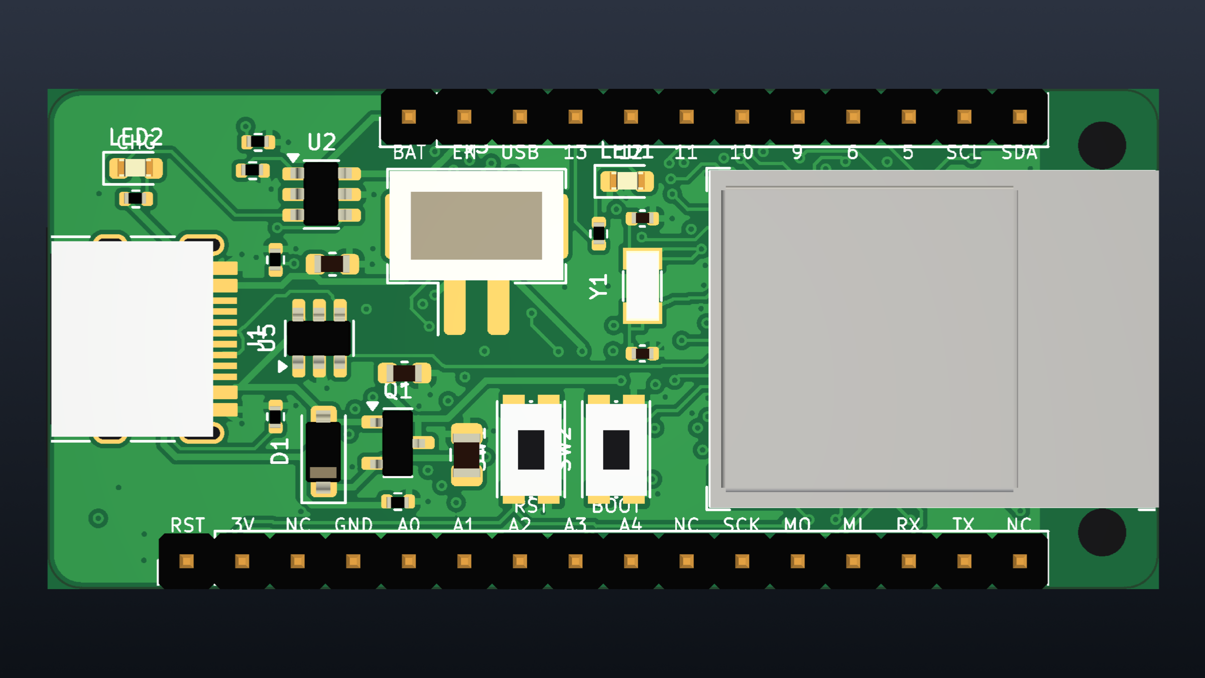 |  |
Top side
Bottom side
CUT=I).| F.Cu | In1 (GND plane) |
|---|---|
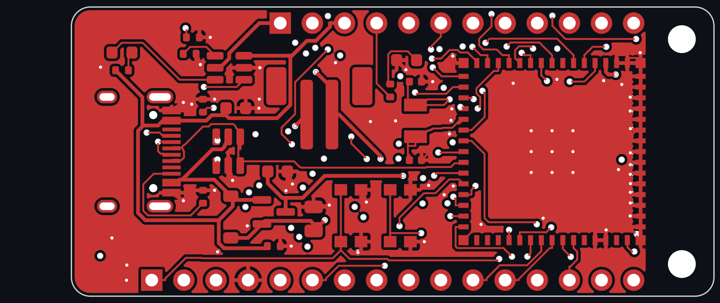 | 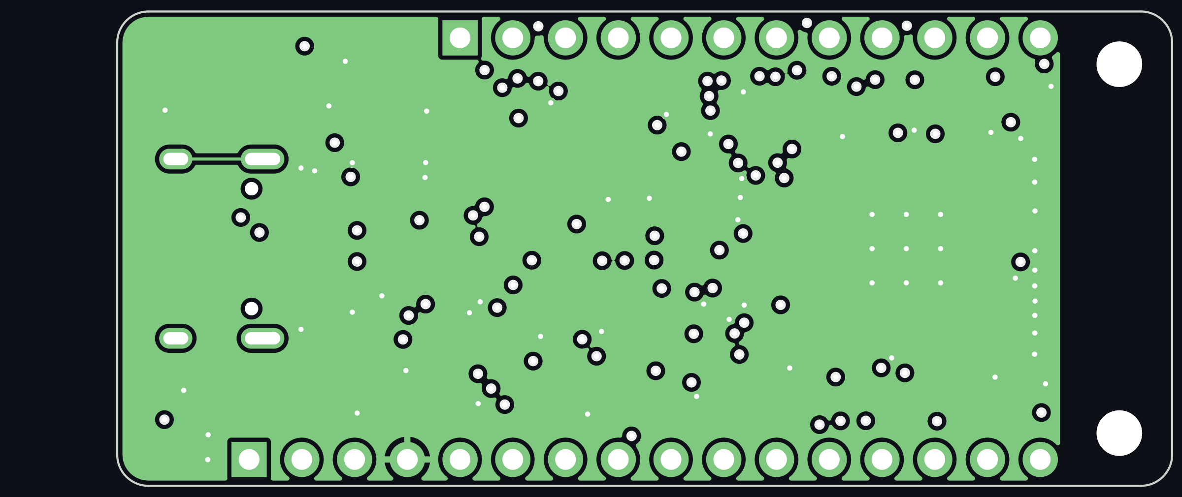 |
| In2 | B.Cu |
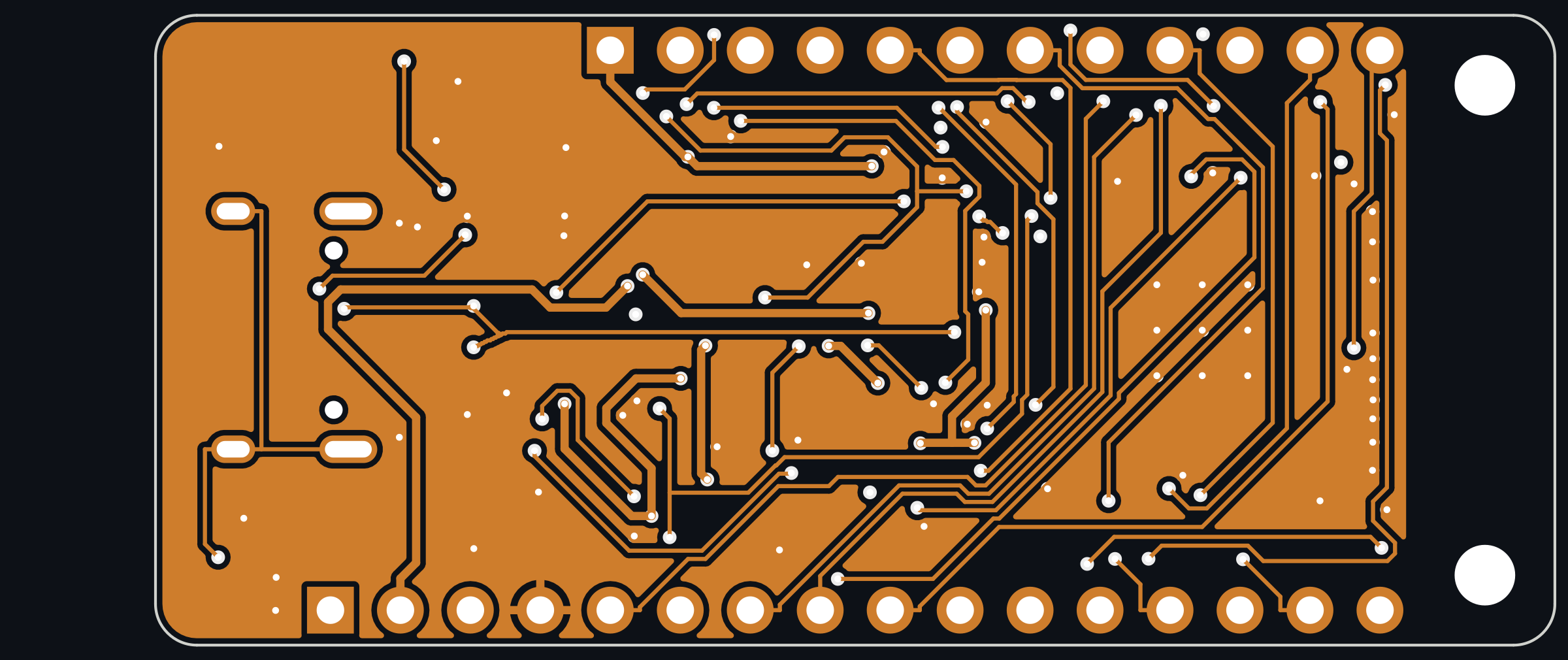 | 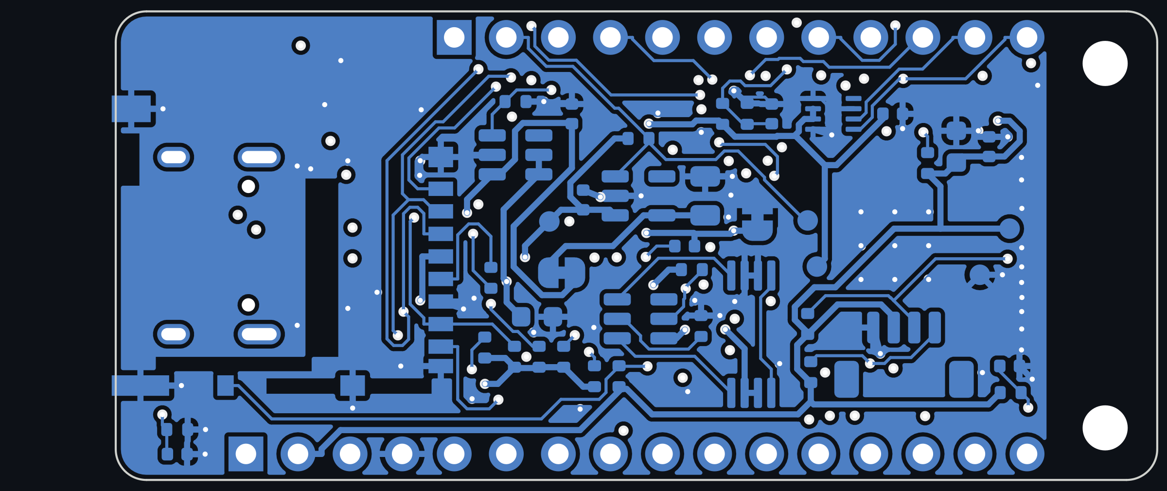 |
Layout decisions:
../README.md R8).Set for a standard 4-layer prototype service (JLCPCB/PCBWay class): track/space 0.15/0.15 mm signal (fab minimum is typically 0.09–0.1 mm), 0.3 mm power, via 0.5 mm pad / 0.25 mm drill, hole-to-copper 0.2 mm, copper-to-edge 0.25 mm. Check the 0.25 mm drill against your fab's standard (not premium) capability before ordering.
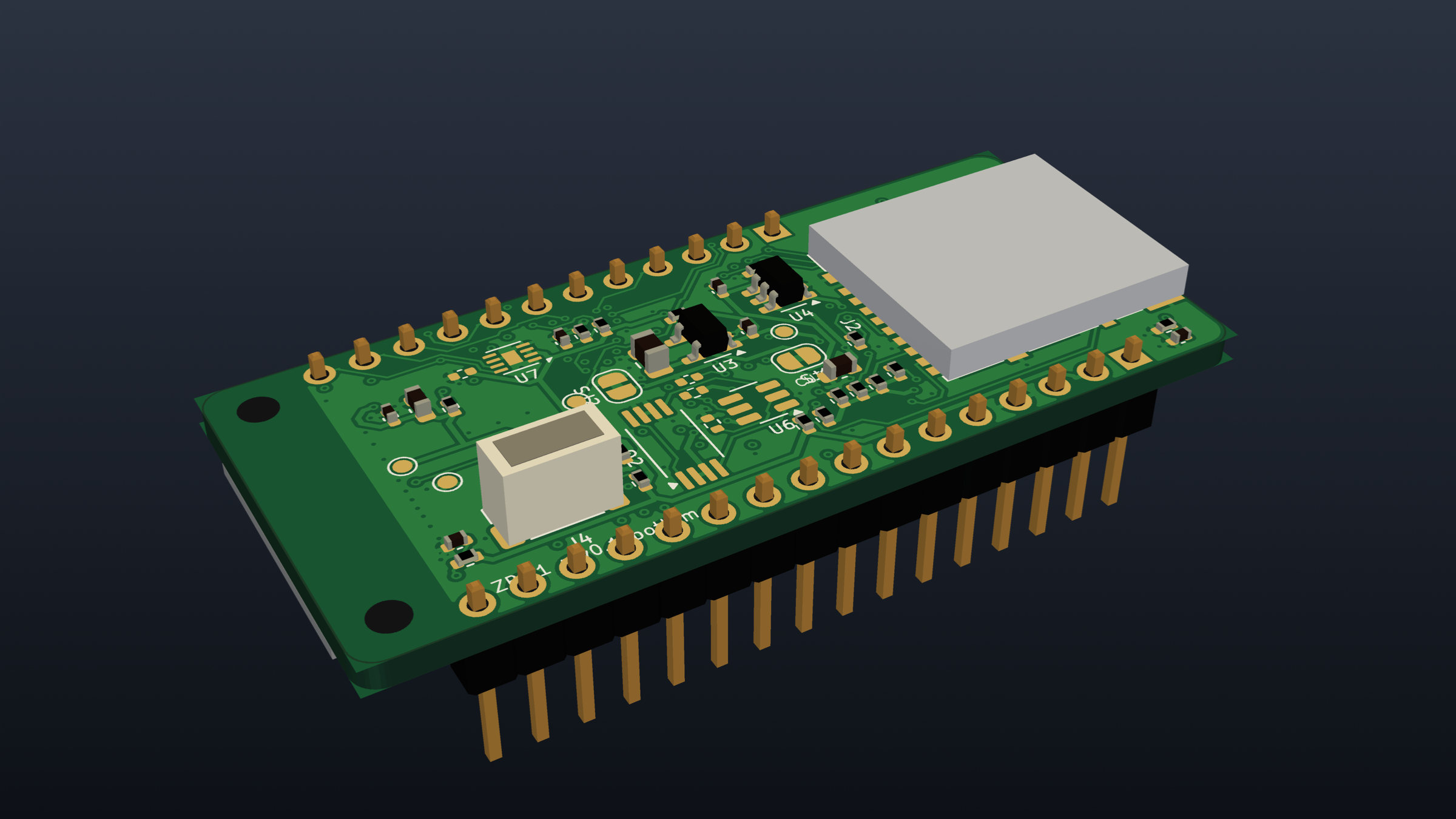
3d/zb1.step contains the bare board and every fitted part:
The envelopes are correct in footprint position and outline size, so they are good enough for designing an enclosure, but they are not detailed parts. DNP parts are omitted. The renders overlay the board's real copper, mask, ENIG pads and silkscreen, composited from the KiCad layer plots, onto the STEP geometry.
Report: reports/drc.rpt, KiCad 7.0.11 DRC run on the saved board with all zones
refilled.
| Category | Count | Severity | Status |
|---|---|---|---|
| Unconnected items | 0 | error | every net is routed |
| Clearance, hole clearance, shorts, track width, annular ring, keep-out violations by copper | 0 | error | — |
| Courtyard overlap: M2 holes H3/H4 vs module U1 and the header rows | 4 | error | waiver. These are the screw-head courtyards of the antenna-end Feather holes, with exactly the same geometry as Adafruit's ESP32-S3 Feather. The holes are NPTH, with no copper. Use nylon screws or bottom-side standoffs only. |
| Items not allowed: H3/H4 courtyard inside the module footprint's antenna keep-out | 2 | error | waiver for the same holes: no copper and no parts sit in the keep-out; only the screw-head clearance circle touches it. Drop H3/H4 entirely if you prefer a strictly clean report. |
| Copper to board edge: microSD shell tabs (J2 pad 11) | 2 | error | waiver. The socket is edge-mounted by design: its slot is at the board edge. The tabs are GND. |
| Silkscreen overlap / clipped by mask / clipped by edge | 73 | warning | cosmetic. Mostly footprint outlines on dense 0402 areas and the USB-C/microSD outlines that cross the edge. The fab clips silk to mask (--subtract-soldermask). |
| Footprint differs from library copy | 21 | warning | expected: these footprints were given envelope 3D models or the DNP attribute in the board |
How routing was completed. Three routing tools were involved, in order:
scripts/complete.py). A small net-aware A* router on a 0.05 mm grid
routes a few nets first and locks them:
Freerouting is deterministic for a given input, but small input changes reshuffle its result. So
scripts/best_of.py tries three pre-route sets and keeps the best. Result:
| Pre-route set | Unconnected |
|---|---|
| A | 1 |
| B | 0 (used) |
| C | 1 |
What still needs a human before ordering (beyond the checklist in §7):
scripts/zb1_design.py     single source of truth: every part, footprint, value, MPN, pin -> net
scripts/gen_libs.py       project symbols + module footprint/3D model
scripts/gen_models.py     envelope STEP bodies for parts without library models
scripts/gen_schematic.py  zb1.kicad_sch (A2, seven blocks), verified by verify_netlist.py
scripts/gen_pcb.py        outline, fixed placements, greedy courtyard-clearing placement of the rest,
                          antenna keep-out, module no-track area          -> build/zb1_placed.kicad_pcb
scripts/route.py          GND fan-out vias, Specctra DSN (with In1 GND plane), Freerouting -> build/zb1.ses
scripts/finish.py         session import, GND pours on 4 layers, silkscreen, zone fill, DRC
scripts/export.py         Gerbers/drill/pos/BOM, PDFs, STEP, layer plots, surface textures, renders
scripts/texture.py        mask/copper/ENIG/silk composite of the KiCad layer plots
scripts/render3d.py       STEP -> OpenCASCADE -> VTK off-screen renders
To change the circuit:
zb1_design.py../build.sh.To move parts, edit FIXED / TARGET in gen_pcb.py.
Toolchain used (2026-10-19):
-Dzb1.opt.seconds), set to 600 s here.KiCad 8/9 will open and upgrade the project.
zb1.kicad_pro in KiCad, run DRC, and finish or clean up anything listed in §5.../README.md §10.| Qty | Value | Footprint | References |
|---|---|---|---|
| 8 | 10k | Resistor_SMD:R_0402_1005Metric | R4, R9, R10, R11, R12, R13, R14, R25 |
| 4 | 1M | Resistor_SMD:R_0402_1005Metric | R5, R6, R8, R22 |
| 4 | 1uF | Capacitor_SMD:C_0402_1005Metric | C4, C10, C15, C16 |
| 3 | 100k | Resistor_SMD:R_0402_1005Metric | R7, R16, R17 |
| 3 | 100nF | Capacitor_SMD:C_0402_1005Metric | C7, C13, C14 |
| 3 | 10uF | Capacitor_SMD:C_0603_1608Metric | C1, C6, C11 |
| 2 | 18pF | Capacitor_SMD:C_0402_1005Metric | C8, C9 |
| 2 | 22uF | Capacitor_SMD:C_0805_2012Metric | C3, C5 |
| 2 | 4.7k | Resistor_SMD:R_0402_1005Metric | R18, R19 |
| 2 | 5.1k | Resistor_SMD:R_0402_1005Metric | R1, R2 |
| 2 | M2 | MountingHole:MountingHole_2.2mm_M2 | H3, H4 |
| 1 | 1.07k | Resistor_SMD:R_0402_1005Metric | R3 |
| 1 | 100 | Resistor_SMD:R_0402_1005Metric | R23 |
| 1 | 1k | Resistor_SMD:R_0402_1005Metric | R21 |
| 1 | 2.2k | Resistor_SMD:R_0402_1005Metric | R20 |
| 1 | 2k | Resistor_SMD:R_0402_1005Metric | R24 |
| 1 | 32.768kHz 12.5pF | Crystal:Crystal_SMD_3215-2Pin_3.2x1.5mm | Y1 |
| 1 | 33 | Resistor_SMD:R_0402_1005Metric | R15 |
| 1 | 3V3 | TestPoint:TestPoint_Pad_D1.0mm | TP4 |
| 1 | 4.7nF | Capacitor_SMD:C_0402_1005Metric | C12 |
| 1 | 4.7uF | Capacitor_SMD:C_0603_1608Metric | C2 |
| 1 | B5819W | Diode_SMD:D_SOD-123 | D1 |
| 1 | BATT JST-PH | Connector_JST:JST_PH_B2B-PH-SM4-TB_1x02-1MP_P2.00mm_Vertical | J3 |
| 1 | BOOT | Button_Switch_SMD:SW_Push_1P1T_NO_CK_KMR2 | SW2 |
| 1 | BQ21040DBVR | Package_TO_SOT_SMD:SOT-23-6 | U2 |
| 1 | CHG orange | LED_SMD:LED_0603_1608Metric | LED2 |
| 1 | DMG3415U | Package_TO_SOT_SMD:SOT-23 | Q1 |
| 1 | DW01A | Package_TO_SOT_SMD:SOT-23-6 | U6 |
| 1 | ESP32-S3-MINI-1-N8 | zb1:ESP32-S3-MINI-1 | U1 |
| 1 | FS8205A | Package_SO:TSSOP-8_4.4x3mm_P0.65mm | Q2 |
| 1 | Feather 12 | Connector_PinHeader_2.54mm:PinHeader_1x12_P2.54mm_Vertical | J6 |
| 1 | Feather 16 | Connector_PinHeader_2.54mm:PinHeader_1x16_P2.54mm_Vertical | J5 |
| 1 | GND | TestPoint:TestPoint_Pad_D1.0mm | TP5 |
| 1 | I_MEAS | Jumper:SolderJumper-2_P1.3mm_Bridged_RoundedPad1.0x1.5mm | SJ1 |
| 1 | MAX17048G+T10 | Package_DFN_QFN:TDFN-8-1EP_2x2mm_P0.5mm_EP0.8x1.2mm | U7 |
| 1 | PROT bypass | Jumper:SolderJumper-2_P1.3mm_Bridged_RoundedPad1.0x1.5mm | SJ2 |
| 1 | RESET | Button_Switch_SMD:SW_Push_1P1T_NO_CK_KMR2 | SW1 |
| 1 | RT9080-33GJ5 | Package_TO_SOT_SMD:SOT-23-5 | U3 |
| 1 | STEMMA-QT | Connector_JST:JST_SH_BM04B-SRSS-TB_1x04-1MP_P1.00mm_Vertical | J4 |
| 1 | TPS22917DBVR | Package_TO_SOT_SMD:SOT-23-6 | U4 |
| 1 | TP_EN | TestPoint:TestPoint_Pad_D1.0mm | TP1 |
| 1 | USB-C | Connector_USB:USB_C_Receptacle_HRO_TYPE-C-31-M-12 | J1 |
| 1 | USBLC6-2SC6 | Package_TO_SOT_SMD:SOT-23-6 | U5 |
| 1 | USER red | LED_SMD:LED_0603_1608Metric | LED1 |
| 1 | VBAT | TestPoint:TestPoint_Pad_D1.0mm | TP2 |
| 1 | VSYS | TestPoint:TestPoint_Pad_D1.0mm | TP3 |
| 1 | microSD push-push | Connector_Card:microSD_HC_Hirose_DM3AT-SF-PEJM5 | J2 |
JGAguado/LIA
Low-power pet tracking platform built around Meshtastic and LoRa mesh networking

dark-Phoenix2077/voidboard
custom esp32 devboard with extensive power management and a built-in IMU

HYLDAIC/Flagshep-V1_Audio-Player
A high fidelity semi-portable audio player student project with provided PCB files, 3D files and Code

MorgenWebDigital/airquality
A battery-powered indoor air quality monitor. Real CO₂ from a photoacoustic sensor, VOC and NOx, temperature, humidity and ambient light, shown on a 2.13" e-paper display and sent over Bluetooth LE.

nikolaus018/dji-fcc-esp32
ESP32-S3 firmware that switches a DJI N1 remote to FCC mode over USB (replaces the Android app)


justinlindh/bramble
Privacy-first LoRa mesh networking for ESP32-S3, built with ESP-IDF

It measures 50.8 × 22.9 mm and has 4 copper layers, 1.6 mm thick.
71 parts, built around the ESP32-S3-MINI-1-N8, DW01A, MAX17048G+T10 and RT9080-33GJ5. The full list of its parts is on this page, with links to each part's symbol and footprint where PCBKit's library has them.
From the danindiana/zemizdat repository on GitHub, at the commit this page was made from: the board is 05_hardware/zb1/cad/zb1.kicad_pcb and its schematic 05_hardware/zb1/cad/zb1.kicad_sch. PCBKit opens the board in the browser, with nothing to install.
Its repository publishes it under the Apache-2.0 licence: you may reuse it on that licence's terms (keep the author's notice, and for a copyleft licence share your changes alike).