
4 layers234 × 84 mm
Main panel
google/mozc-devices
Circuit diagrams and firmware source code for Gboard DIY keyboards
234 parts3kApache-2.0

 DabbiSabbi/macropad1
A hackpad that that uses F13-19
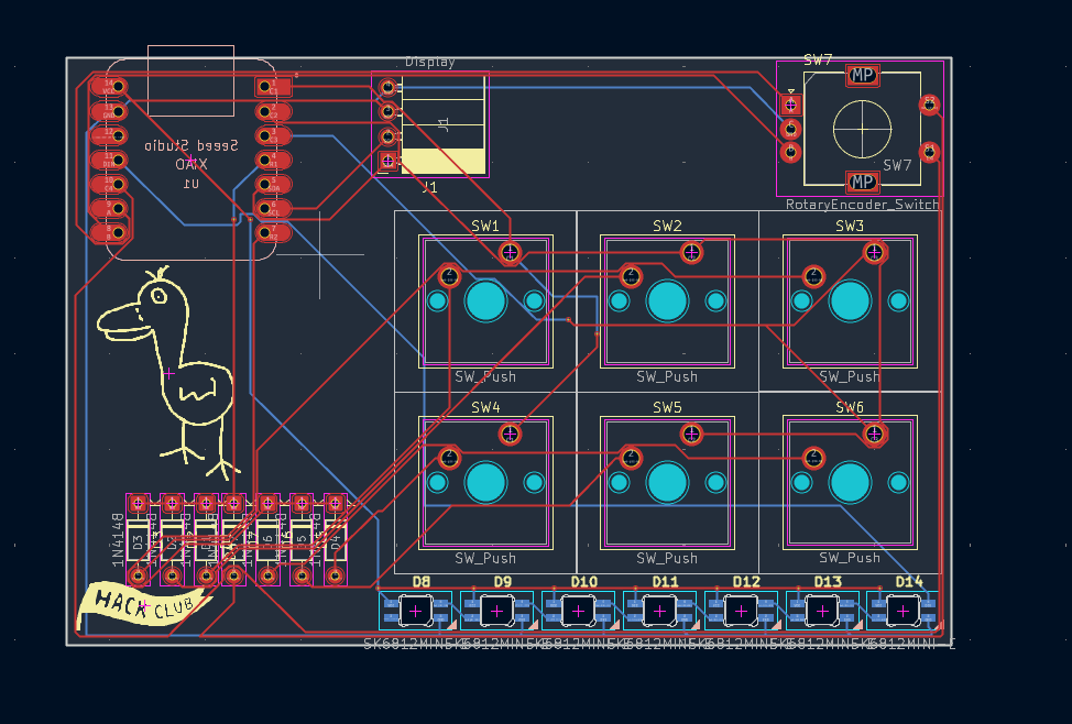
My Hackpad is an open-source printed circuit board by DabbiSabbi, from the DabbiSabbi/macropad repository on GitHub. It is a 2-layer board of 92.5 × 61.5 mm with 25 parts on 28 nets, routed with 232 tracks and 11 vias.
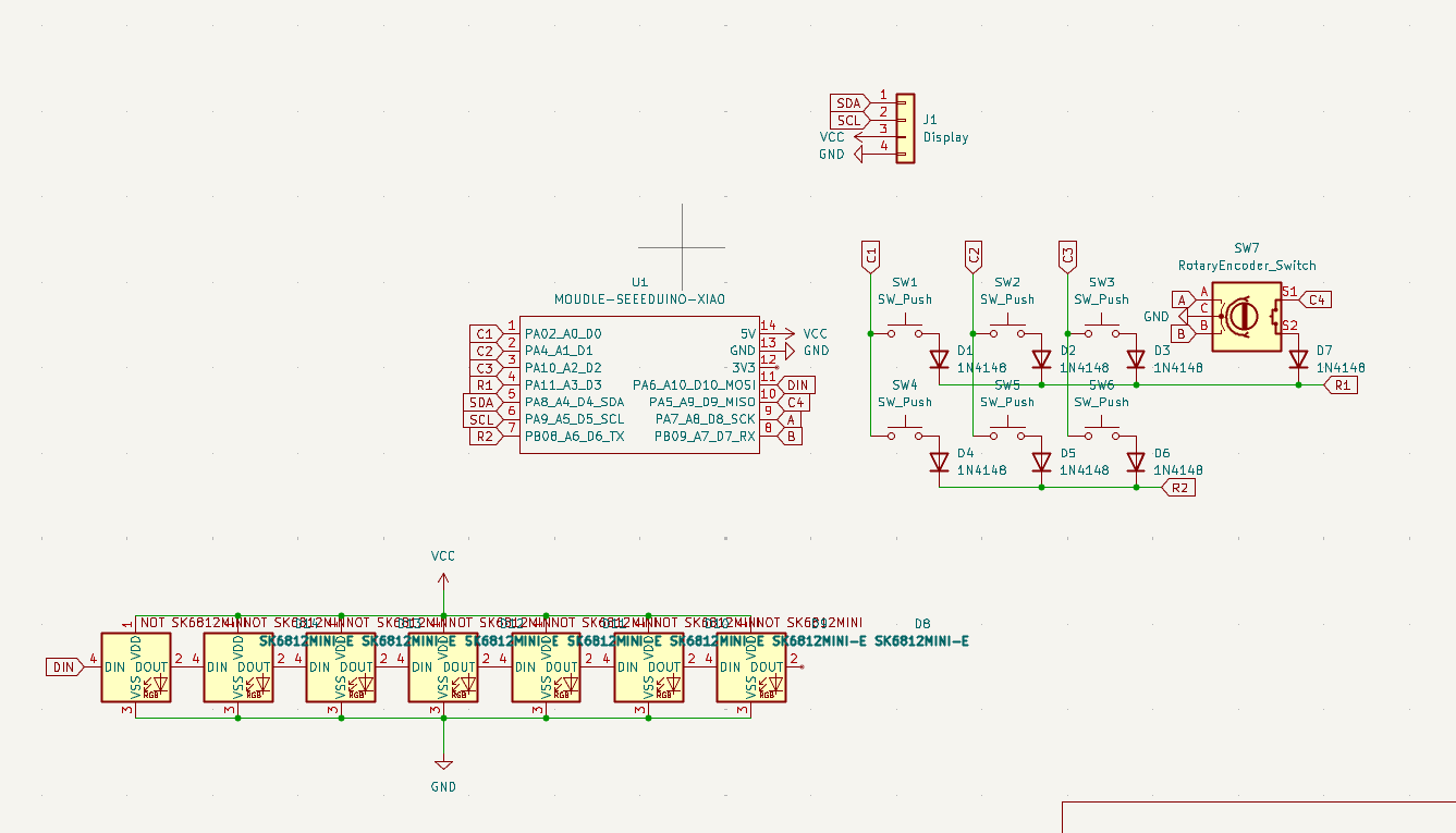
It is built around the SK6812MINI-E. Its parts include 14 diodes, 7 switches, 1 IC and 1 connector.
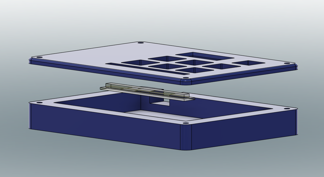
The body is in 3 parts, a lid, base and diffuser, The diffuser is meant to be printed in a clear material such as clear PETG.
| Part | Quantity |
|---|---|
| Seeed XIAO RP2040 | 1 |
| 1N4148 Diodes | 7 |
| MX-Style switches | 6 |
| EC11E Rotary encoders | 1 |
| 0.91 inch OLED display | 1 |
| SK6812 MINI-E LEDs | 6 |
| DSA keycaps | 6 |
| M3x16mm screws | 4 |
| M3x5mx4mm heatset inserts | 4 |
This was made for Hackpad
| Qty | Value | Footprint | References |
|---|---|---|---|
| 7 | 1N4148 | Diode_THT:D_DO-35_SOD27_P7.62mm_Horizontal | D1, D2, D3, D4, D5, D6, D7 |
| 7 | SK6812MINI-E | footprints:SK6812MINI-E_fixed | D8, D9, D10, D11, D12, D13, D14 |
| 6 | SW_Push | Button_Switch_Keyboard:SW_Cherry_MX_1.00u_PCB | SW1, SW2, SW3, SW4, SW5, SW6 |
| 2 | LOGO | LOGO | G***, G*** |
| 1 | Display | Connector_PinSocket_2.54mm:PinSocket_1x04_P2.54mm_Horizontal | J1 |
| 1 | MOUDLE-SEEEDUINO-XIAO | footprints:XIAO-Generic-Hybrid-14P-2.54-21X17.8MM | U1 |
| 1 | RotaryEncoder_Switch | Rotary_Encoder:RotaryEncoder_Alps_EC11E-Switch_Vertical_H20mm | SW7 |
It measures 92.5 × 61.5 mm and has 2 copper layers, 1.6 mm thick.
25 parts, built around the SK6812MINI-E. The full list of its parts is on this page, with links to each part's symbol and footprint where PCBKit's library has them.
From the DabbiSabbi/macropad repository on GitHub, at the commit this page was made from: the board is PCB/My-Hackpad.kicad_pcb and its schematic PCB/My-Hackpad.kicad_sch. PCBKit opens the board in the browser, with nothing to install.
Its repository states no licence, so its author keeps all rights: ask DabbiSabbi before reusing the design.
google/mozc-devices
Circuit diagrams and firmware source code for Gboard DIY keyboards

Bastardkb/Dilemma
The Dilemma is a vertical stagger low-profile keyboard with mods.

Pwnsat/FlatSat
Flatsat v1.0 is a hardware based platform for aerospace cybersecurity research

adamws/kicad-kbplacer
KiCad plugin for automatic keyboard's key placement and routing

imchipwood/dumbpad
Simple 4x4 numpad with rotary encoder. Powered by QMK via ATmega32u4 Pro Micro

makerforgetech/modular-biped
An open source framework for creating a bipedal modular companion robot.

