2 layers58.8 × 55.4 mm
Retrocution usb hub
CoryParsnipson/electronics-experiments
Educational and experimental PCB designs for Raspberry pi related products and peripherals
35 parts1MIT

 CoryParsnipson/electronics-experiments1
Educational and experimental PCB designs for Raspberry pi related products and peripherals
Max98357-amp is an open-source printed circuit board by CoryParsnipson, from the CoryParsnipson/electronics-experiments repository on GitHub, published under the MIT licence. It is a 2-layer board of 24.1 × 58.2 mm with 18 parts on 14 nets, routed with 92 tracks and 4 vias.
Its parts include 8 connectors, 4 capacitors, 2 resistors, 1 IC and 1 switch. It belongs with the audio and music boards of this library.
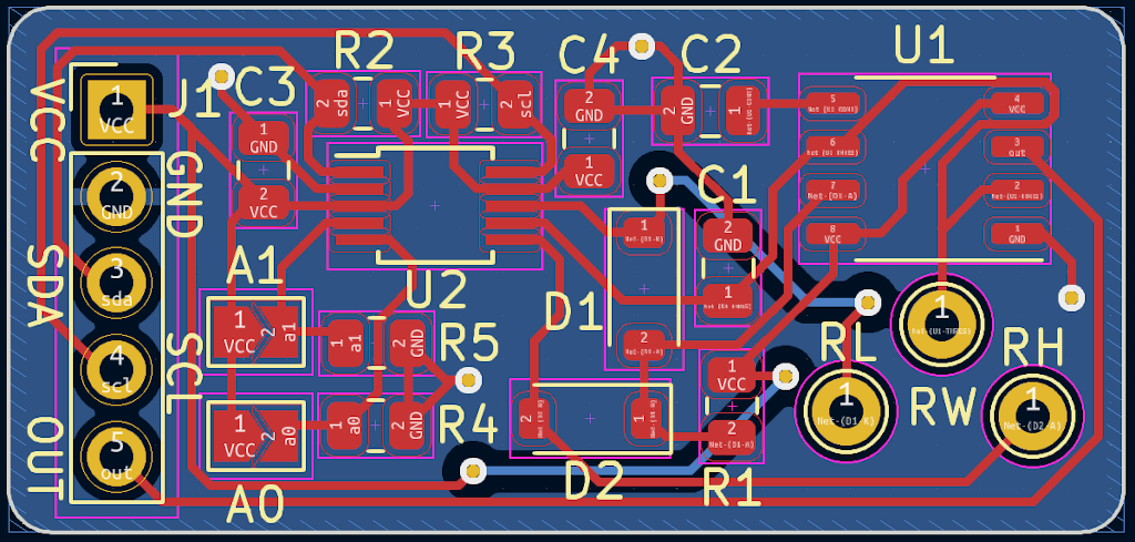
This is a hardware pwm signal generator using a 555 timer. The design used here is one that uses two diodes attached to both ends of a potentiometer to make the duty cycle adjustable without changing the frequency. A twist on the usual design is that this project also uses a digital potentiometer (a.k.a. digipot) so that the duty cycle can be adjusted programmatically with a microcontroller via an I2C interface.
The purpose of this project is to provide digital access to an adjustable PWM signal to dim an lcd backlight driver. (See ap5726-lcd-backlight-driver.) The output signal of this project can be fed into the enable signal of an lcd backlight driver.
This project is not recommended for real usage. This is not a very good way to generate a PWM signal compared to other methods. See Post Mortem for more detailed information.
Current version: KiCAD 7.0.2.
This was originally made with KiCAD 7.0.2.
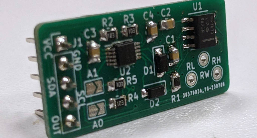
A good explanation of how 555-timers work and how they operate in astable-multivibrator mode can be found at How to Generate PWM Signal using 555 Timer IC, also listed as [1] in References. The author does a good job of explaining the functional logic and how it works. Basically, a 555-timer can be used to emit signal pulses at very specific, user-settable delays. This is known as "monostable" mode. A 555-timer can also be induced to oscillate like a clock signal by using feedback loops. This mode of operation is known as "astable" because it changes value by itself and "multi-vibrator" because it assumes different values.
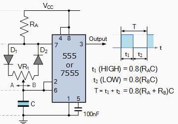
Unfortunately, the author of [1] doesn't explain the PWM oscillator circuit in detail and really drops the ball at the end. I found a second page, 555 Circuits Part 1, ([2] under References) that describes creating a PWM generator step-by-step starting from 555-timer astable mode. I am basing this project's circuit off of the "Fully Independent 555 Oscillator". [2] goes into much more detail about the circuit design. These two webpages together, I feel, are a very good primer into 555 circuits.
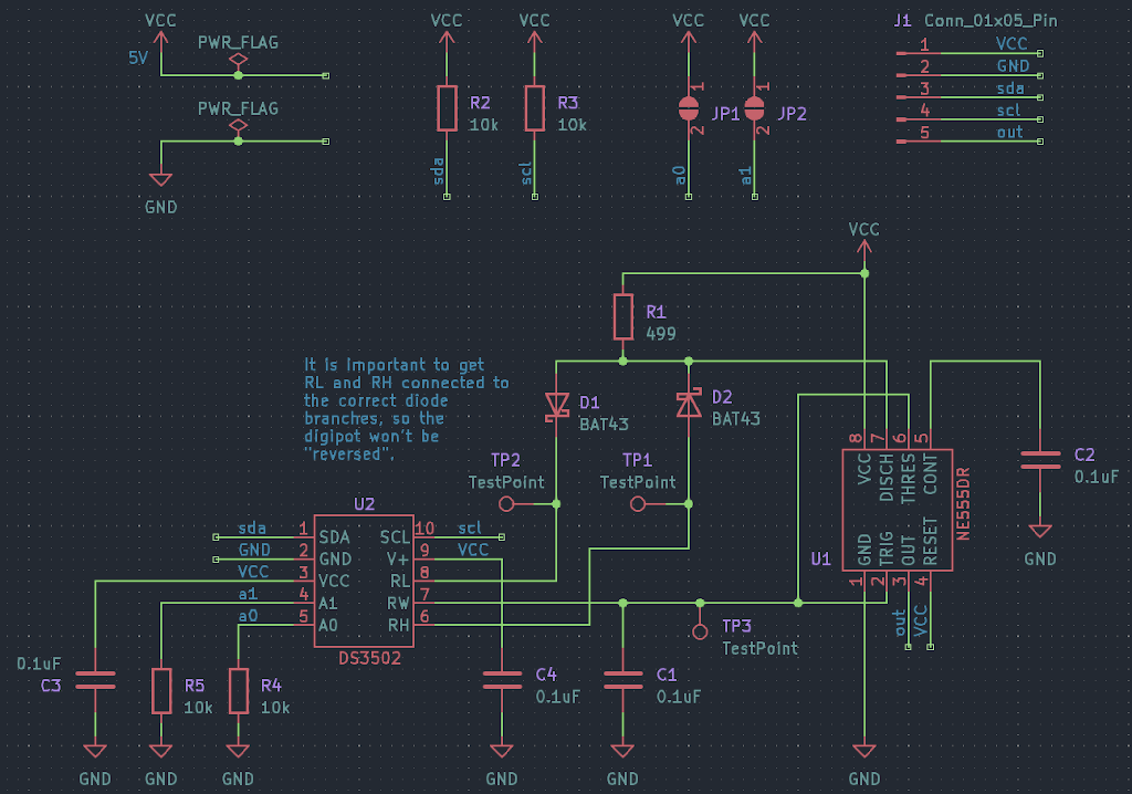
The schematic was created by following the block diagram for the frequency independent 555-oscillator shown above. The DS3502 digipot is incorporated using the layout copied from the Adafruit breakout board. The SDA and SCL signals require 10k pull up resistors. The A0 and A1 pins are hooked up to solder jumper pads for configurability. To change the I2C address, bridge the solder pins. The digipot also needs decoupling capacitors close to the V+ and Vin pins.
As explained by [1] and [2], the frequency and duty cycle that the oscillator will assume can be adjusted by selecting values for the three main components, the capacitor C, the fixed resistor RA, and the potentiometer RB.

The duty cycle is solely determined by the ratio of both resistors. Where RA is the "top" resistor, in series with the capacitor charging path, and RB is the bottom resistor, in series with the discharge path. As you can see from the formula, the duty cycle can theoretically go up to 100%, but RA is constraining the lower limit. We want this to be small.
These resistor values can give us a minimum 5% duty cycle. This most likely is not enough to completely turn off the LEDs. That is something I wish I knew before I started, that this particular design is not able to achieve a full duty cycle range. (As a note, other methods of generating PWM signals can achieve a full 0-100% duty cycle range.)
The last component to select is the value of the charging/discharging capacitor. This capacitor has the most influence on frequency.
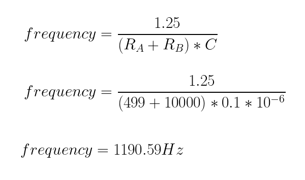
The frequency we want should be <= 2 kHz, because this design is being made to control the enable signal of the AP5726 white led driver, and that chip is expecting an unfiltered PWM signal to be under 2 kHz. Going with the previous select resistor values, and a capacitor that is 0.1 uF, we get an expected frequency of 1190 Hz.
NOTE: One can still use this circuit and insert different valued components to change the duty cycle and frequency. This PCB layout uses 0805 (2012 metric) surface mount size resistors and capacitors.
The 1.25 constant in this formula comes from the inverse of 0.8, which itself had been changed from its original value of 0.693. This value is the ln(2), derived from some sort of manipulation of an exponential growth/decay formula. The site [2] mentions that the value was changed to 0.8 to account for using diodes with lower than usual threshold voltage. The derivation of this is not something I was able to find or come up with myself... In my experiment, this does not accurately reflect the empirically observed frequency that ended up being half the estimated value.
I was able to take that measurement and deduce that in my real component, the 1.25 factor is actually 0.546 for some reason.
This was done by taking the frequency measurement here and plugging that back into the frequency formula to solve for the "1.25" term. To get back to an expected 1190 Hz, one could halve the capacitor value to use 0.05 uF (50 nF) for a frequency of 1040.10 Hz. This is if 5V input voltage is used. If 3.3V will be used, the capacitor value may have to be reduced by a factor of 30%. (See Post Mortem for more information about this...)
The TLC555CDR 555-timer is recommended for it's small form factor, low pin count, and ability to run at 3.3V.
The DS3502 was used because it was available in breakout board form from Adafruit. However, in retrospect, the MCP4561T-103E (Alternative digipot with low wiper resistance) is a much better part with similar features. (See Post Mortem for why this is.) This PCB layout is not designed to work with the MCP4561T-103E as-is. The pins differ between the two chips.
This design needs fast switching small signal diodes, preferably with a low threshold voltage. The BAT34W-TP schottky diodes were chosen.
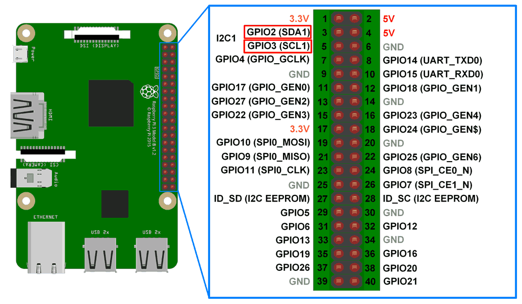
The SDA and SCL pins of the PCB should be hooked up to the corresponding SDA and SCL pins of your microcontroller of choice. I used a Raspberry Pi 3, as depicted in the above picture. One also needs to make sure the I2C peripheral is enabled and reboot the RPi. And that's all for the interfacing setup!
One may use the available raspberry pi package "i2c-tools":
sudo apt-get install i2c-tools
This package provides a basic way to talk to I2C devices, using i2cdetect, i2cset, and i2cget.
#> i2cdetect -y 1
     0  1  2  3  4  5  6  7  8  9  a  b  c  d  e  f
00:          -- -- -- -- -- -- -- -- -- -- -- -- --
10: -- -- -- -- -- -- -- -- -- -- -- -- -- -- -- --
20: -- -- -- -- -- -- -- -- 28 -- -- -- -- -- -- --
30: -- -- -- -- -- -- -- -- -- -- -- -- -- -- -- --
40: -- -- -- -- -- -- -- -- -- -- -- -- -- -- -- --
50: -- -- -- -- -- -- -- -- -- -- -- -- -- -- -- --
60: -- -- -- -- -- -- -- -- 68 -- -- -- -- -- -- --
70: -- -- -- -- -- -- -- --

#> i2cget -y 1 0x28 0x00
0x40

#> i2cset -y 1 0x28 0x00 0x00                 # set the digipot to 0 (shortest duty cycle)
#> i2cset -y 1 0x28 0x00 0x7F                 # set the digipot to 127 (longest duty cycle)
If everything is working correctly, you should see a device on I2C port 1 address 0x28. (This may differ if you've bridged the A0 and/or A1 pins). Upon intial start-up you should see a read to the digipot register will return 0x40, which is halfway to 128, corresponding to a 50% duty cycle.
This design was originally going to be used together with an ap5726-lcd-backlight-driver to dim LEDs. Unfortunately, this design was not performing to expectations.
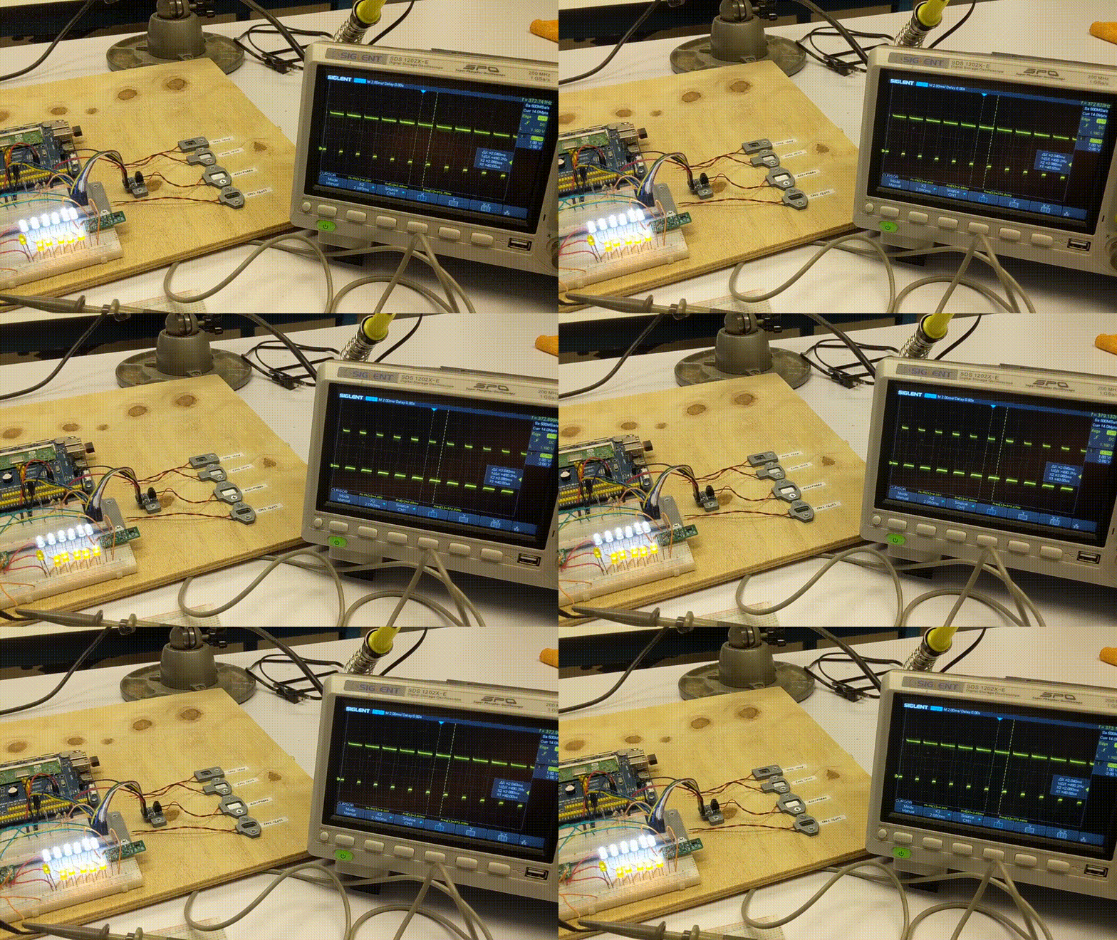
Here is a video of me writing the min and max values to the digipot and the subsequent duty cycle generated by those values. The difference is not very noticeable...
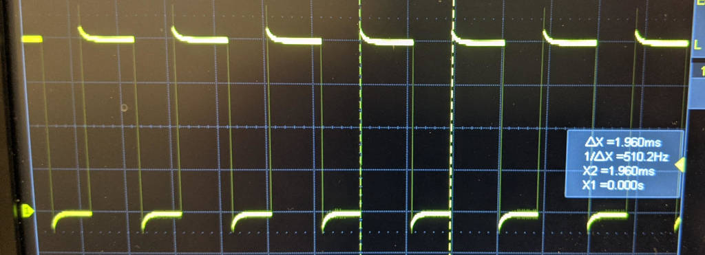
I measured the duty cycle of both min and max values. First, here is the total period measurement:
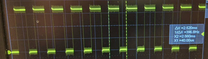
My oscilloscope shows 398 Hz frequency or 2.520 ms period. Here is the minimum duty cycle:
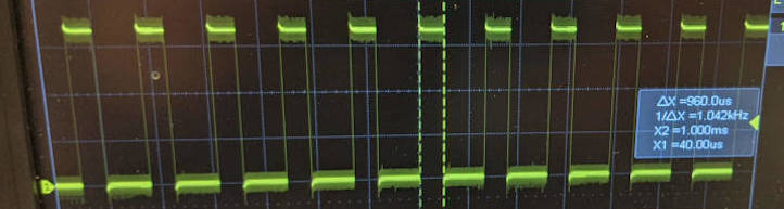
The high pulse is 960 us long. This corresponds to a duty cycle of 38.1%! Terrible!
And the max duty cycle:
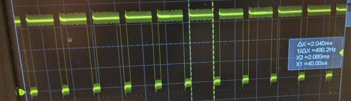
The high pulse is 2.040 ms long. This corresponds to a duty cycle of 81%! Also terrible!
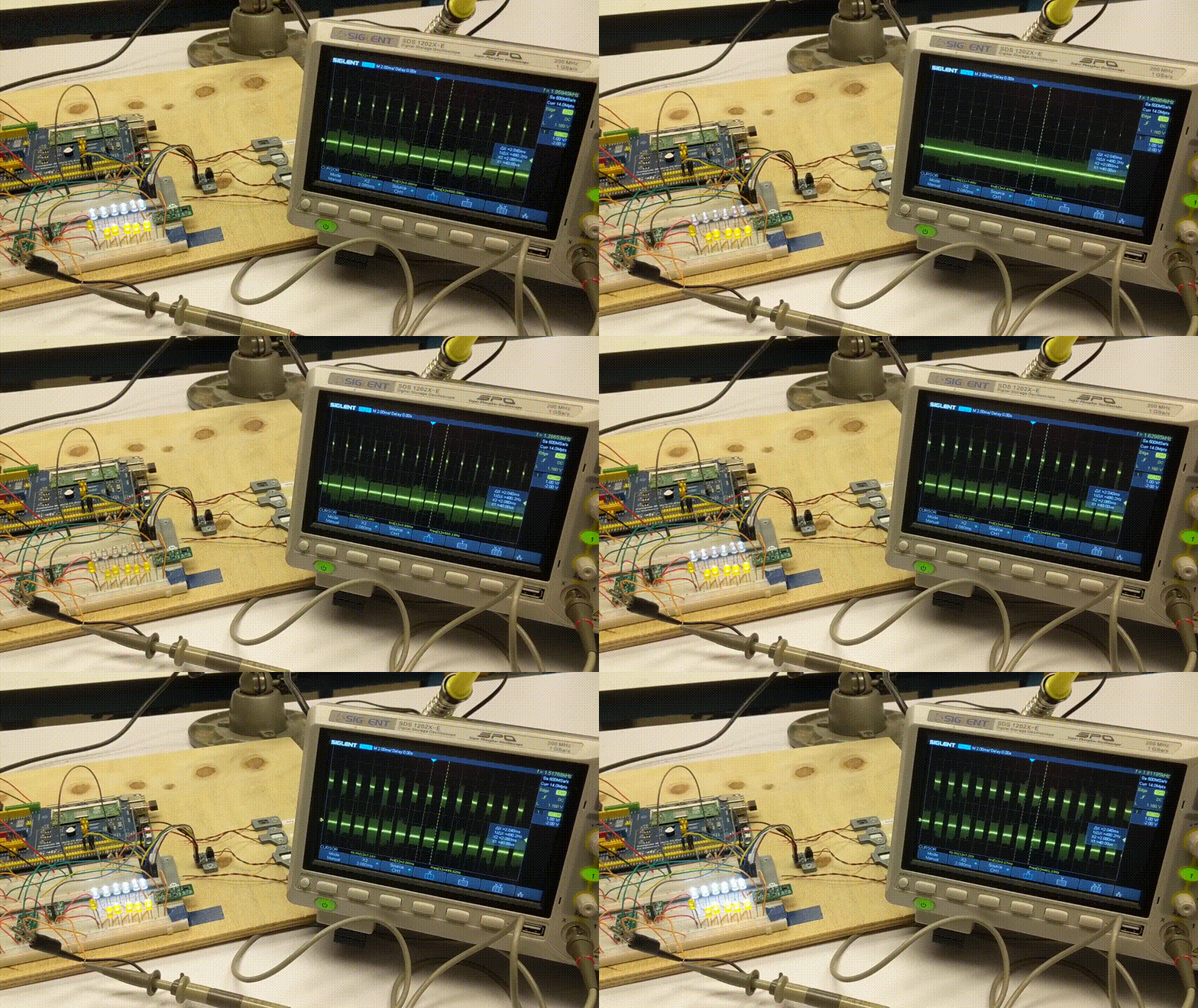
For reference, here is a pwm cycle coming from a Raspberry Pi, that is able to go fully from 0 to 100% duty cycle:
Using a fudge factor of 0.8 instead of 0.692 (a.k.a. the ln(2)) is due to adding in fast switching diodes that have a threshold voltage of about 0.4-0.5 volts instead of 0.7 volts. In the real world, the diode characteristics can still vary enough to make the actual frequency different. After putting together this circuit in real life, the frequency of the PWM signal was observed to be around 520 Hz @ 5V VCC and a 1190 Hz signal was expected.
The frequency is also dependent on input voltage. So while the frequency was in the 500 Hz range at 5V, it gets lower at 3.3V. At such voltage, the frequency was recorded to be around 390 Hz.
It is unknown exactly why there is a discrepancy...
The DS3502 digipot has a nominal wiper resistance of 5000 ohms. This is quite large and cannot be ignored when doing frequency calculations. This large resistance shows up on both the charge and discharge timing, reducing the duty cycle range from 5% - 100% to around 30% - 80%. This is not good, and the qualitative difference in LED brightness is barely perceptable. The lower duty cycle range is especially important to being able to dim the LEDs to near shutoff.
If I disconnect the digipot and use a 10k resistor and a short circuit to connect the RL, RW, and RH pins into the 555-timer, I can see what the actual duty cycle limits are without the digipot characteristics getting in the way.
If I put the 10k resistor across RW and RH, this will simulate minimum duty cycle:
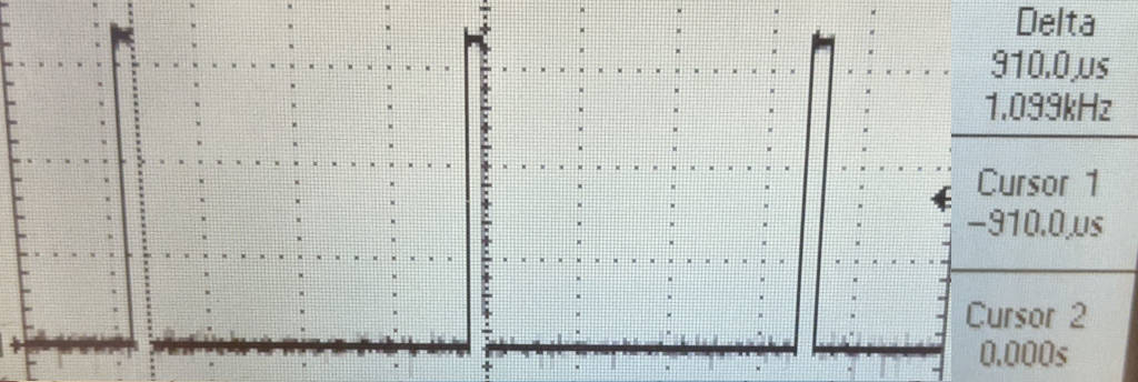
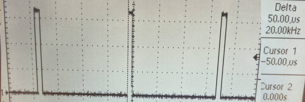
The period here is 910 us and the duty cycle is high for 50 us. That corresponds to a 5.47% duty cycle. Very close to the calculated value!
Putting the 10k resistor across RW and RL will be equivalent to maximum duty cycle:
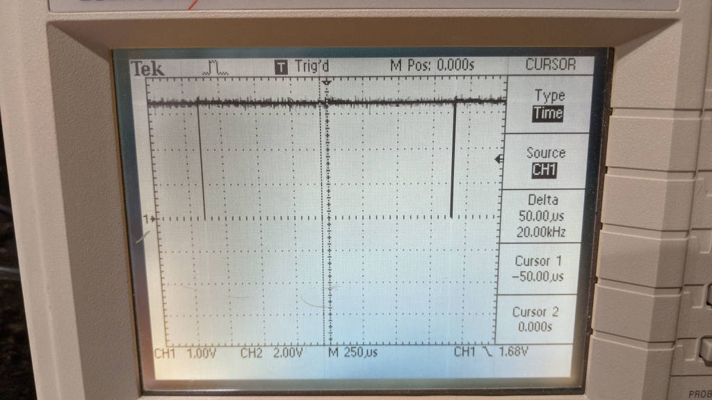
This is very, very close to 100%. So this is pretty definitive evidence that the 5000 ohm wiper resistance is messing things up.
This design uses too many expensive components. The DS3502 (and similar) digipots are about $1.80 USD. This design also requires a 555-timer, 2 expensive diodes, 5 resistors, and 4 ceramic capacitors. Overall, the design costs around $5-7 USD for this single functional block. (Compare to using an ATTiny25, which is ~$1 USD and aside from 2 pull up resistors for I2C signals, is the only part you need.)
There are a few things one can implement to improve upon this design, however, none of them change the fact that it is unsuitable for real world usage.
Replace DS3502 digipot with one that has smaller wiper resistance
For instance, the MCP4561T-103E not only has a nominal wiper resistance of 75 ohms but it has 257 steps instead of the DS3502's 127. This will probably improve the duty cycle range drastically. Combined with using a slightly smaller charging resistor (RA), you could get to the theoretical 5% minimum duty cycle.
Implement negative resistance op amp circuit
Negating the wiper resistance of a digipot has been thought of before. One may attempt to use an op amp to create a circuit that would negate the wiper resistance of the digipot. Article here.
This was not done for this project. An alternate method will be chosen to dim the LEDs.
Use a microcontroller to generate the PWM signal. Using an extra wire from a Raspberry Pi and generating a PWM signal from it works really well, at the cost of requiring an entire Raspberry Pi and an extra wire to generate the signal. If one wants to embed an microcontroller into the PCB so that the user will not have to supply their own microcontroller, one can use an ATTiny25. This microcontroller does not require any external components and can run off 3.3V. So the user simply needs to incorporate the footprint onto the PCB and then write fireware to configure I2C, non-volatile memory storage, and enable PWM generation on one of the pins.
Here is a good explanation of how a microcontroller is able to generate a PWM signal.
Use multi-op-amps in an astable vibrator configuration. This is similar to using a 555-timer, except the design is more complicated. The benefits are that the frequency will be more stable with the op-amps and the wiper resistance of the digipot will not matter because you can use a comparator op-amp to adjust to the digipot's output range.
| Qty | Value | Footprint | References |
|---|---|---|---|
| 4 | Conn_01x02_Male | Connector_PinHeader_2.54mm:PinHeader_1x02_P2.54mm_Vertical | J2, J3, J4, J8 |
| 2 | Conn_01x01_Male | Connector_PinHeader_2.54mm:PinHeader_1x01_P2.54mm_Vertical | J5, J6 |
| 2 | FerriteBead | Resistor_SMD:R_0603_1608Metric | FB1, FB2 |
| 1 | 0.1uF | Capacitor_SMD:C_0603_1608Metric | C2 |
| 1 | 10uF | Capacitor_SMD:C_0603_1608Metric | C1 |
| 1 | 200k | Resistor_SMD:R_0603_1608Metric | R1 |
| 1 | 220pF | Capacitor_SMD:C_0603_1608Metric | C3 |
| 1 | 220pf | Capacitor_SMD:C_0603_1608Metric | C4 |
| 1 | 680k | Resistor_SMD:R_0603_1608Metric | R2 |
| 1 | AS01808AO-mount | project:AS01808AO-mount | S1 |
| 1 | Conn_01x07_Male | Connector_PinHeader_2.54mm:PinHeader_1x07_P2.54mm_Vertical | J1 |
| 1 | MAX98357 | project:MAX98357-TQFN16-T1633+4 | U1 |
| 1 | Screw_Terminal_01x02 | TerminalBlock_Phoenix:TerminalBlock_Phoenix_PT-1,5-2-3.5-H_1x02_P3.50mm_Horizontal | J7 |
CoryParsnipson/electronics-experiments
Educational and experimental PCB designs for Raspberry pi related products and peripherals

CoryParsnipson/electronics-experiments
Educational and experimental PCB designs for Raspberry pi related products and peripherals

CoryParsnipson/electronics-experiments
Educational and experimental PCB designs for Raspberry pi related products and peripherals

CoryParsnipson/electronics-experiments
Educational and experimental PCB designs for Raspberry pi related products and peripherals

CoryParsnipson/electronics-experiments
Educational and experimental PCB designs for Raspberry pi related products and peripherals


VoronDesign/Voron-Hardware
Cool Hardware designed by the Voron Design group


hackclub/OnBoard
💡 Join 1,000 teenagers and make your first PCB with a $100 grant!

VoronDesign/Voron-Tap
Tap is a nozzle-based z-probe for the V2 and Trident printer designs. The entire toolhead moves to trigger an optical switch. Tap offers many advantages:

Luos-io/luos_engine
Open-source and real-time orchestrator for cyber-physical-systems, to easily design, test and deploy embedded applications and digital twins.


Twotoz/C5VRX
Ultra-minimal, zero-CPU 5.8 GHz analog FPV video receiver using ESP32-C5 Wi-Fi 6 PHY MODEM_DIAG, BitScrambler WBFM demodulation & resistor DAC CVBS
It measures 24.1 × 58.2 mm and has 2 copper layers, 1.6 mm thick.
18 parts. The full list of its parts is on this page, with links to each part's symbol and footprint where PCBKit's library has them.
From the CoryParsnipson/electronics-experiments repository on GitHub, at the commit this page was made from: the board is max98357-amp/max98357-amp.kicad_pcb and its schematic 555-timer-pwm-with-digipot/555-timer-pwm-with-digipot.kicad_sch. PCBKit opens the board in the browser, with nothing to install.
Its repository publishes it under the MIT licence: you may reuse it on that licence's terms (keep the author's notice, and for a copyleft licence share your changes alike).