2 layers55.1 × 112.5 mm
Cw optics cwside
colinoflynn/phase-modulation-sca
Resources to demonstrate phase modulation leakage including over JTAG
44 parts8

 colinoflynn/phase-modulation-sca8
Resources to demonstrate phase modulation leakage including over JTAG
Cw isolator powered is an open-source printed circuit board by colinoflynn, from the colinoflynn/phase-modulation-sca repository on GitHub. It is a 2-layer board of 87.6 × 72.6 mm with 68 parts on 70 nets, routed with 465 tracks and 66 vias.
It is built around the ADE-1+, TBA 1-0511E and BSS138, with the FDN340P among its other parts. Its parts include 28 resistors, 19 capacitors, 10 connectors, 5 ICs and 2 diodes. It belongs with the interfaces and adapters boards of this library.


This repository is a companion for the T-CHES Paper "Phase Modulation Side Channels: Jittery JTAG for On-Chip Voltage Measurements". You can see a current version on the T-CHES Server.
If referencing the paper, please reference the T-CHES publication. As the Volume 4 is not fully published, the following can be used until the full reference is available:
@article{PhaseModulationCO24,
     author=  {Colin O'Flynn},
     title =  {Phase Modulation Side Channels: Jittery JTAG for On-Chip Voltage Measurements},
     volume=  {2024},
     url   =  {https://tches.iacr.org/index.php/TCHES/article/view/11797},
     DOI   =  {10.46586/tches.v2024.i4.382-424},
     number=  {4},
     journal= {IACR Transactions on Cryptographic Hardware and Embedded Systems},
     year  =  {2024},
     month =  {Sep.},
pages = {382–424} }The following is a very brief summary of the above paper:
At CHES 2023, a paper entitled JitSCA was presented. This paper presented the idea that because the propogation delay through a digital device depends on the voltage, a signal (such as a clock) transmitted from a digital device actually encodes in the "jitter" of that clock the voltage supply.
The paper in this repo expands on this to first demonstrate that we could call that a simple phase modulation. A demonstration board using isolators (both optical & ic-based are tested) is setup, which looks like this:
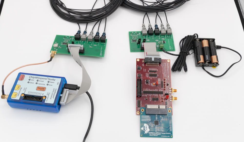
The point of this is that all analog signals (should) be removed, leaving only the timing (phase) information (NB: note similar tests were done in the JitSCA work, there are some extensions but this section is primarily confirming the prior work). Because this is all done using the ChipWhisperer hardware, we can easily compare a classic shunt-based measurement (using a normal analog signal) with our phase-based measurement (after the optical isolators). The top waveforms (in green) are using the optical isolator board, the bottom waveforms (in blue) are with a shunt resistor and ADC.
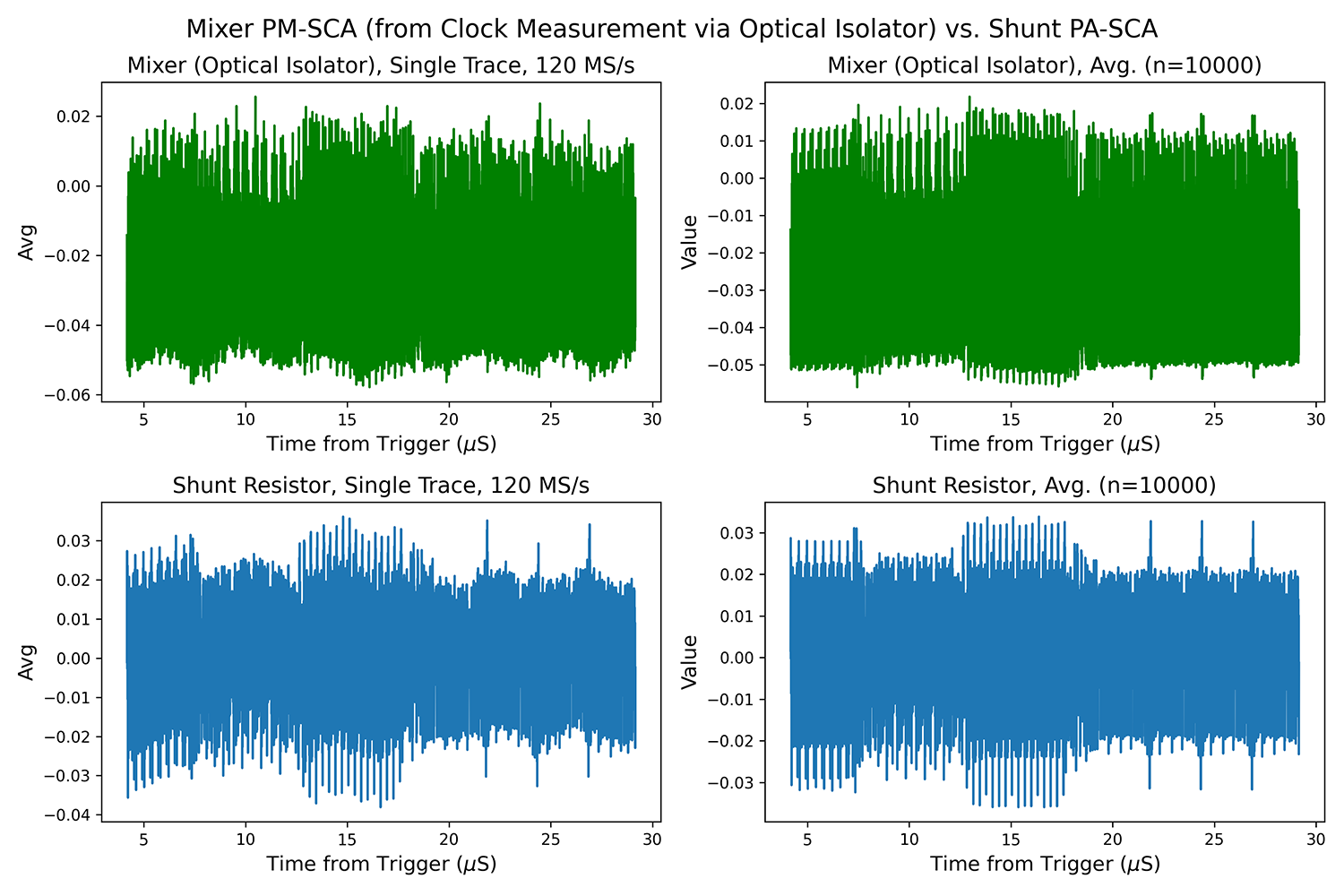
Visually it looks shockingly similar! The phase measurement based test only has optically isolated digital signals. In the paper I described a lot of comparisons done to confirm the leakage is present (and to also compare to prior I/O-pin leakage work).
It is also successful for a CPA attack, being only slightly noisier. You could use any clock source from the device, such as an uSD card SCLK line as the jitter source. But we can go further:
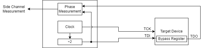
The second part of the paper includes another idea: if we can use digital paths for side channels, why not use JTAG? JTAG contains a "bypass mode", which if we enable bypass mode lets us route a clock across the target. The setup is something like this:
Here is an example of a side channel trace measured with a JTAG port, again compared to the same target using a shunt resistor:
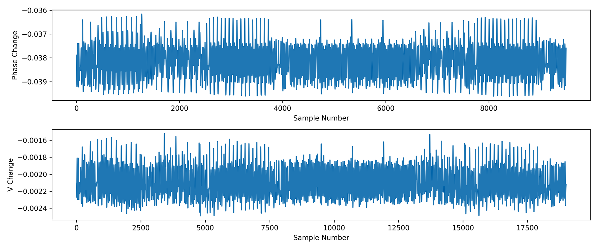
This has a few interesting results:
Another variation of this uses something called "fault sensitivity analysis". In this case we actually use the fact that if we adjust the timing of our signals such that faults are "about" to occur, we can measure the liklihood of faults at a given instance of time to again create analog (power-like) waveforms.
This is noisier and takes more traces, as you basically have a 1-bit ADC. But again, it is suprisingly effective.
The repository is a companion to the paper, and also includes all the code as well as hardware designs for the tools used.
More details of building the tools is forthcoming, but see the details in the paper for now.
| Qty | Value | Footprint | References |
|---|---|---|---|
| 12 | 1R | Resistor_SMD:R_0603_1608Metric | R3, R4, R5, R6, R7, R8, R9, R10, R11, R12, R13, R14 |
| 8 | 100n | Resistor_SMD:R_0603_1608Metric | C4, C6, C7, C10, C11, C12, C13, C16 |
| 6 | 2u2 | Resistor_SMD:R_0603_1608Metric | C2, C3, C5, C9, C14, C15 |
| 5 | DNM | Resistor_SMD:R_0603_1608Metric | R16, R20, R21, R22, R24 |
| 4 | SMA | Connector_Coaxial:SMA_Molex_73251-1153_EdgeMount_Horizontal | J7, J8, J9, J10 |
| 3 | 10K | Resistor_SMD:R_0603_1608Metric | R17, R18, R23 |
| 3 | 10n | Resistor_SMD:R_0603_1608Metric | C17, C18, C19 |
| 2 | 1K | Resistor_SMD:R_0603_1608Metric | R19, R28 |
| 2 | 22u/16V | Capacitor_SMD:C_0805_2012Metric | C1, C8 |
| 2 | 51R | Resistor_SMD:R_0603_1608Metric | R26, R27 |
| 2 | 5K1 | Resistor_SMD:R_0603_1608Metric | R1, R2 |
| 2 | Conn_02x03_Odd_Even | Connector_PinHeader_2.54mm:PinHeader_2x03_P2.54mm_Vertical | J5, J6 |
| 2 | Conn_02x10_Odd_Even | Connector_IDC:IDC-Header_2x10_P2.54mm_Vertical | J3, J4 |
| 2 | L | Inductor_SMD:L_0805_2012Metric | L1, L2 |
| 2 | MAX22164FAEE+T | Package_SO:SSOP-16_3.9x4.9mm_P0.635mm | IC1, IC2 |
| 1 | 100R | Resistor_SMD:R_0603_1608Metric | R29 |
| 1 | 200R | Resistor_SMD:R_0603_1608Metric | R15 |
| 1 | ADE-1+ | RF_Mini-Circuits:Mini-Circuits_CD542_LandPatternPL-052 | U3 |
| 1 | BSS138 | Package_TO_SOT_SMD:SOT-23 | Q1 |
| 1 | Conn_01x03 | Connector_PinHeader_2.54mm:PinHeader_1x03_P2.54mm_Vertical | J1 |
| 1 | FDN340P | Package_TO_SOT_SMD:SOT-23 | Q2 |
| 1 | LD1117S33TR_SOT223 | Package_TO_SOT_SMD:SOT-223-3_TabPin2 | U2 |
| 1 | LED | LED_THT:LED_D3.0mm | D2 |
| 1 | LED | LED_THT:LED_D5.0mm | D1 |
| 1 | TBA1-0511E | Converter_DCDC:Converter_DCDC_TRACO_TBA1-xxxxE_Single_THT | U1 |
| 1 | USB_C_Receptacle_PowerOnly_6P | Connector_USB:USB_C_Receptacle_GCT_USB4125-xx-x_6P_TopMnt_Horizontal | J2 |
colinoflynn/phase-modulation-sca
Resources to demonstrate phase modulation leakage including over JTAG

colinoflynn/phase-modulation-sca
Resources to demonstrate phase modulation leakage including over JTAG

colinoflynn/phase-modulation-sca
Resources to demonstrate phase modulation leakage including over JTAG

mpkendall/phase-interferometer
A 2(or more)-element phase interferometric direction finder for 433 MHz using a passive phased array

SomethingFourier/SDR-Receiver
Super Heterodyne Direct Conversion Hybrid I/Q SDR Receiver

ngrabbs/ember
Open pvpanel.kicadpro with KiCad 10. The project contains the recovered schematic, routed PCB, project-local footprint libraries, and solar-module STEP model.

mahdi-kh1265/mts-electronics
Analog RF, photodetector, and demodulation electronics for POSM's modulation-transfer spectroscopy (MTS) laser-locking system.

kholia/ConsensusBasedTimeSync
A portable, efficient, passive, consensus based (relative) time synchronization mechanism over radio waves. Cost-effective radio receivers too!

RunningJoke/reactionButton
ReactPod: ESP32-C3 reaction buzzers – firmware, Config App (PWA), tools, hardware


drandyhaas/HaasoscopePro
Affordable 2 GHz 3.2 GS/s 12 bit open-source open-hardware expandable USB real-time oscilloscope
It measures 87.6 × 72.6 mm and has 2 copper layers, 1.6 mm thick.
68 parts, built around the ADE-1+, TBA 1-0511E, BSS138 and FDN340P. The full list of its parts is on this page, with links to each part's symbol and footprint where PCBKit's library has them.
From the colinoflynn/phase-modulation-sca repository on GitHub, at the commit this page was made from: the board is hardware_tools/cw_isolator_powered/cw_isolator_powered.kicad_pcb and its schematic hardware_tools/cw_isolator_powered/cw_isolator_powered.kicad_sch. PCBKit opens the board in the browser, with nothing to install.
Its repository states no licence, so its author keeps all rights: ask colinoflynn before reusing the design.