2 layers15.9 × 25 mm
IMU
abstractfoundry/lumicube-boards
PCB and firmware design files for some of the LumiCube components
26 parts

 ckemere/usb-imu
USB IMU for camera rigs: BNO055 module (STM32F042) and an FE1.1S hub carrier with JST-GH camera ports. KiCad 9.
Hub imu is an open-source printed circuit board by ckemere, from the ckemere/usb-imu repository on GitHub, published under the CERN-OHL-P-2.0 licence. It is a 2-layer board of 21 × 14.4 mm with 19 parts on 36 nets, routed with 130 tracks and 24 vias.
It is built around the STM32F042F6P6, BNO055 and XC6206P332MR. Its parts include 8 capacitors, 5 resistors, 3 ICs, 2 connectors and 1 diode. It belongs with the sensors and measurement boards and the STM32 boards of this library.


A small 2-layer module that stacks onto a USB 2.0 hub board built around the Terminus FE1.1S hub IC, such as these hubs on Amazon. It plugs into one of the hub's downstream ports through a 0.1" 1x4 header and appears on the host as a USB device that bridges to a Bosch BNO055 9-axis IMU over I2C.
| Top | Bottom |
|---|---|
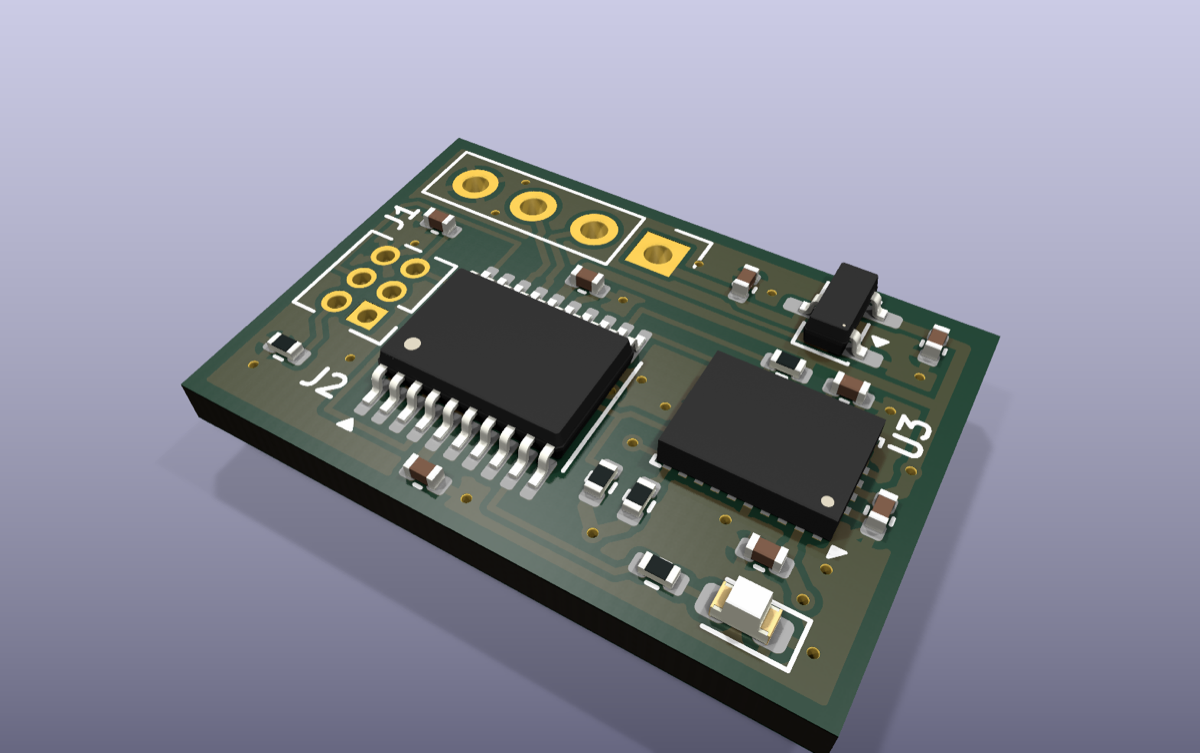 | 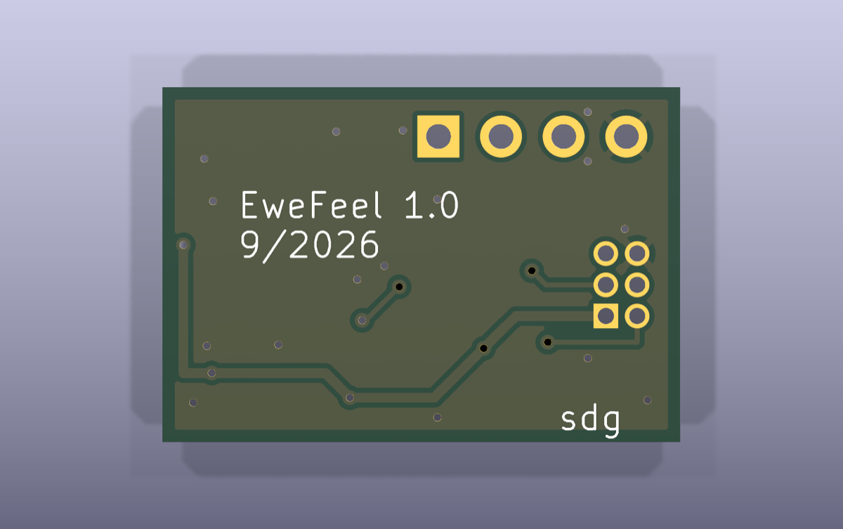 |
The renders come from KiCad's 3D viewer. The J1 and J2 headers are marked do-not-populate (hand-soldered), so they don't appear.
| Assembled module | Next to an FE1.1S hub | Stacked onto the hub |
|---|---|---|
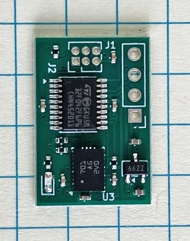 | 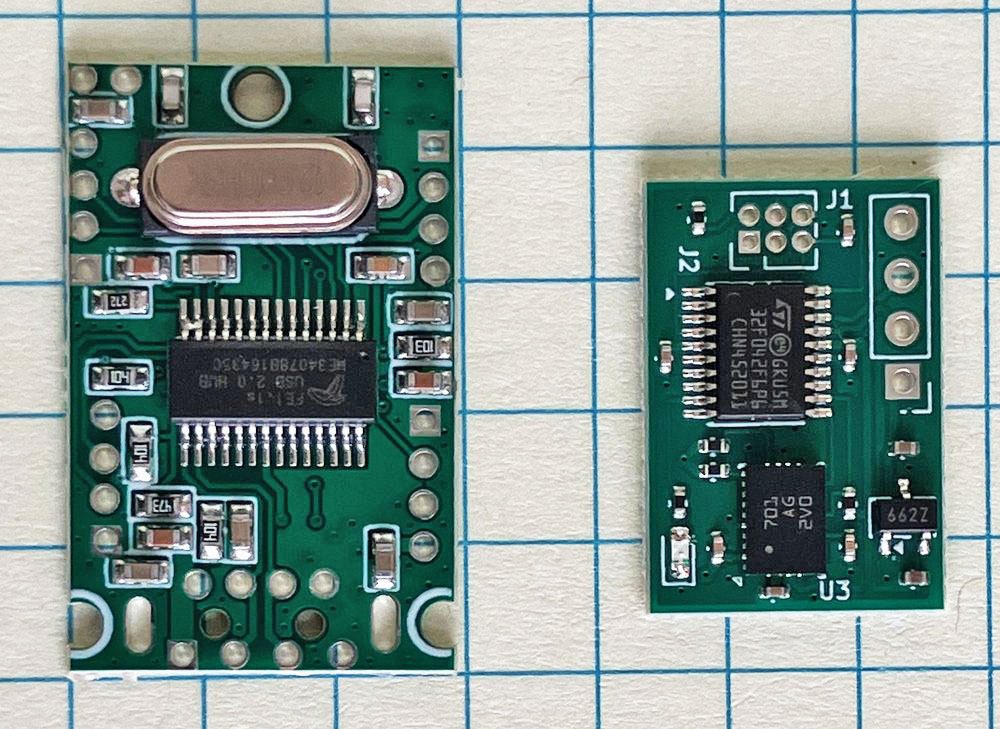 | 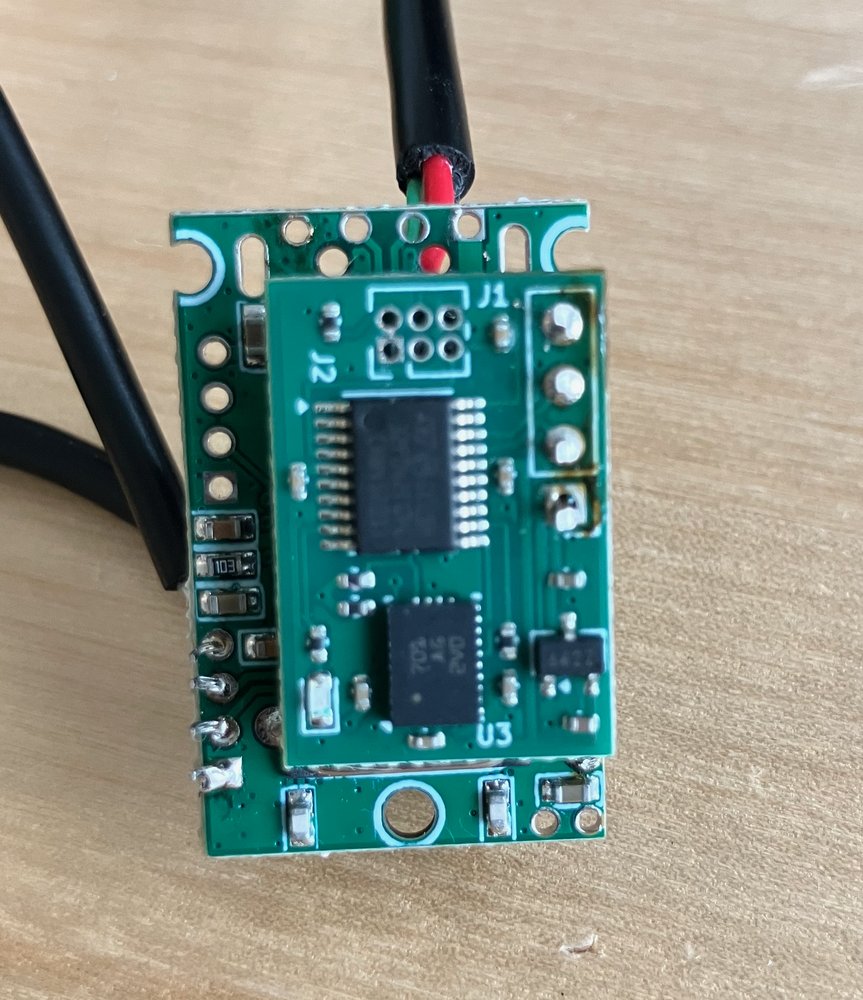 |
| File | What it is |
|---|---|
hub_imu.kicad_pro / .kicad_sch / .kicad_pcb | KiCad project, schematic, layout |
hub_imu.kicad_dru | Custom design rules (see below) |
stage1.svg ... stage5.svg | Layout renders (F.Cu, B.Cu, F.SilkS, Edge.Cuts) after placement, power, USB, signals, pours |
drc_stage1.rpt ... drc_stage5.rpt | DRC report after each stage (drc_stage5.rpt is the final one) |
production/hub_imu.zip | Gerbers and drill files for JLCPCB (from the Fabrication Toolkit plugin) |
images/ | 3D renders and photos used in this README |
| Ref | Part | JLCPCB # (basic) | Role |
|---|---|---|---|
| U1 | STM32F042F6P6 (TSSOP-20) | - (not basic) | Crystal-less USB FS device, USB-to-I2C bridge |
| U2 | BNO055 (LGA-28) | - (not basic) | 9-axis IMU, I2C mode (PS0 = PS1 = GND), address 0x28 (COM3 = GND) |
| U3 | XC6206P332MR (SOT-23-3) | C5446 | 5 V to 3.3 V LDO, 200 mA (pins: 1 VSS, 2 VOUT, 3 VIN), the only heat source |
| J1 | 1x4 2.54 mm header | - (hand-solder) | Connection to the hub |
| J2 | 2x3 1.27 mm header | - (hand-solder) | SWD programming/debug |
| D1 | Red LED, 0603 (KT-0603R) | C2286 | Status LED on PA3 |
| R5 | 1k 0402 | C11702 | LED resistor (~1.3 mA) |
| R3, R4 | 4.7k 0402 | C25900 | I2C pull-ups |
| R1, R2 | 10k 0402 | C25744 | BOOT0 pull-down, BNO055 nRESET pull-up |
| C1 | 1 uF 0402, 25 V X5R | C52923 | LDO input (+5V) |
| C2 | 4.7 uF 0402, 10 V X5R | C23733 | LDO output (+3V3) |
| C3-C8 | 100 nF 0402, 16 V X7R | C1525 | NRST filter; decoupling (U1 VDD, U1 VDDA, U2 VDD, U2 VDDIO, U2 CAP) |
Every assembled part has a JLCPCB Part # field in the schematic and PCB, taken from
JLCPCB's basic parts library. U1, U2, J1 and J2
have the field left blank: the ICs aren't basic parts, and the headers are fitted by hand.
| Pin | Signal |
|---|---|
| 1 | +5V (VBUS) |
| 2 | USB D- |
| 3 | USB D+ |
| 4 | GND |
This pin order has been checked against the hub's downstream-port header.
| Pin | Signal | Pin | Signal |
|---|---|---|---|
| 1 | +3V3 | 2 | BOOT0 |
| 3 | SWDIO | 4 | SWCLK |
| 5 | NRST | 6 | GND |
This is a custom pinout, not a standard ARM SWD connector, so an adapter or cable is needed.
| Function | Pin |
|---|---|
| USB D- / D+ | PA11 / PA12 on pins 17/18. Set SYSCFG_CFGR1.PA11_PA12_RMP, or USB will not enumerate (these pins default to PA9/PA10). |
| I2C1 SDA / SCL | PF0 / PF1 (AF1) |
| BNO055 INT | PA5 (pin 11), EXTI |
| BNO055 nRESET | PA6 (pin 12), drive low to reset (10k pull-up on board) |
| Status LED | PA3 (pin 9), active high, ~1.3 mA (red 0603 LED + 1k) |
| SWD | PA13 / PA14 |
Use the internal HSI48 clock with CRS synced to USB SOF. There is no crystal, and the BNO055's 32 kHz crystal pins are left open (internal clock).
USB_BCu_keepout).U2_BCu_keepout), and no top copper inside U2's pad ring (U2_FCu_interior).hub_imu.kicad_dru)The final DRC (drc_stage5.rpt) shows 0 errors and 0 unconnected pads. The remaining items are
lib_footprint_mismatch warnings on the 0402, SOT-23-3 and LGA footprints. They come from KiCad re-save
rounding on rotated footprints, not from real geometry changes.
ERC reports only lib_symbol_issues, because the hubimu symbols are embedded in the schematic
rather than installed as a library.
Checked against Bosch BST-BNO055-DS000-18 (rev 1.8, Oct 2021); page numbers are the datasheet's own:
There are no open items.
The hardware design is licensed under the CERN Open Hardware Licence v2, Permissive (CERN-OHL-P-2.0).
| Qty | Value | Footprint | References |
|---|---|---|---|
| 6 | 100nF | Capacitor_SMD:C_0402_1005Metric | C3, C4, C5, C6, C7, C8 |
| 2 | 10k | Resistor_SMD:R_0402_1005Metric | R1, R2 |
| 2 | 4.7k | Resistor_SMD:R_0402_1005Metric | R3, R4 |
| 1 | 1k | Resistor_SMD:R_0402_1005Metric | R5 |
| 1 | 1uF | Capacitor_SMD:C_0402_1005Metric | C1 |
| 1 | 4.7uF | Capacitor_SMD:C_0402_1005Metric | C2 |
| 1 | BNO055 | Package_LGA:LGA-28_5.2x3.8mm_P0.5mm | U2 |
| 1 | Red | LED_SMD:LED_0603_1608Metric | D1 |
| 1 | STM32F042F6P6 | Package_SO:TSSOP-20_4.4x6.5mm_P0.65mm | U1 |
| 1 | SWD 2x3 P1.27 | Connector_PinHeader_1.27mm:PinHeader_2x03_P1.27mm_Vertical | J2 |
| 1 | USB 1x4 P2.54 | Connector_PinHeader_2.54mm:PinHeader_1x04_P2.54mm_Vertical | J1 |
| 1 | XC6206P332MR | Package_TO_SOT_SMD:SOT-23-3 | U3 |
It measures 21 × 14.4 mm and has 2 copper layers, 1.6 mm thick.
19 parts, built around the STM32F042F6P6, BNO055 and XC6206P332MR. The full list of its parts is on this page, with links to each part's symbol and footprint where PCBKit's library has them.
From the ckemere/usb-imu repository on GitHub, at the commit this page was made from: the board is hub_imu/hub_imu.kicad_pcb and its schematic hub_cam/hub_cam.kicad_sch. PCBKit opens the board in the browser, with nothing to install.
Its repository publishes it under the CERN-OHL-P-2.0 licence: you may reuse it on that licence's terms (keep the author's notice, and for a copyleft licence share your changes alike).
abstractfoundry/lumicube-boards
PCB and firmware design files for some of the LumiCube components


PetteriAimonen/relaymux
Hardware and firmware for a USB connected relay box

aziraphale/pride-badge-v1
🌈⚡Pride badge PCB with LEDs, STM32, and 3D printed diffuser+case!

Chicken-Fried/STM32-NanoCortex
Ultra-compact USB-C development board powered by STM32F042 (ARM Cortex-M0) with native DFU, ceramic-only LDO power stage & CaveRover branding.

Fluffik214/airsoft-battery-module
This is a USB-C PD charger and cell monitor for a 3S LiPo that lives in an airsoft stock tube. It has one USB-C port.


toyJig/AeroBlinker
Custom PCB w/ KiCAD that reads Receiver Signals to control light flash patterns - Aeronautics Team