4 layers113 × 113.8 mm
ChipOne
chyavanphadke/University-Research-PCB-Design
Specifications: 4 layered PCB that connects a custom designed chip with the Keysight Chip testing device
27 parts

 chyavanphadke/University-Research-PCB-Design
Specifications: 4 layered PCB that connects a custom designed chip with the Keysight Chip testing device
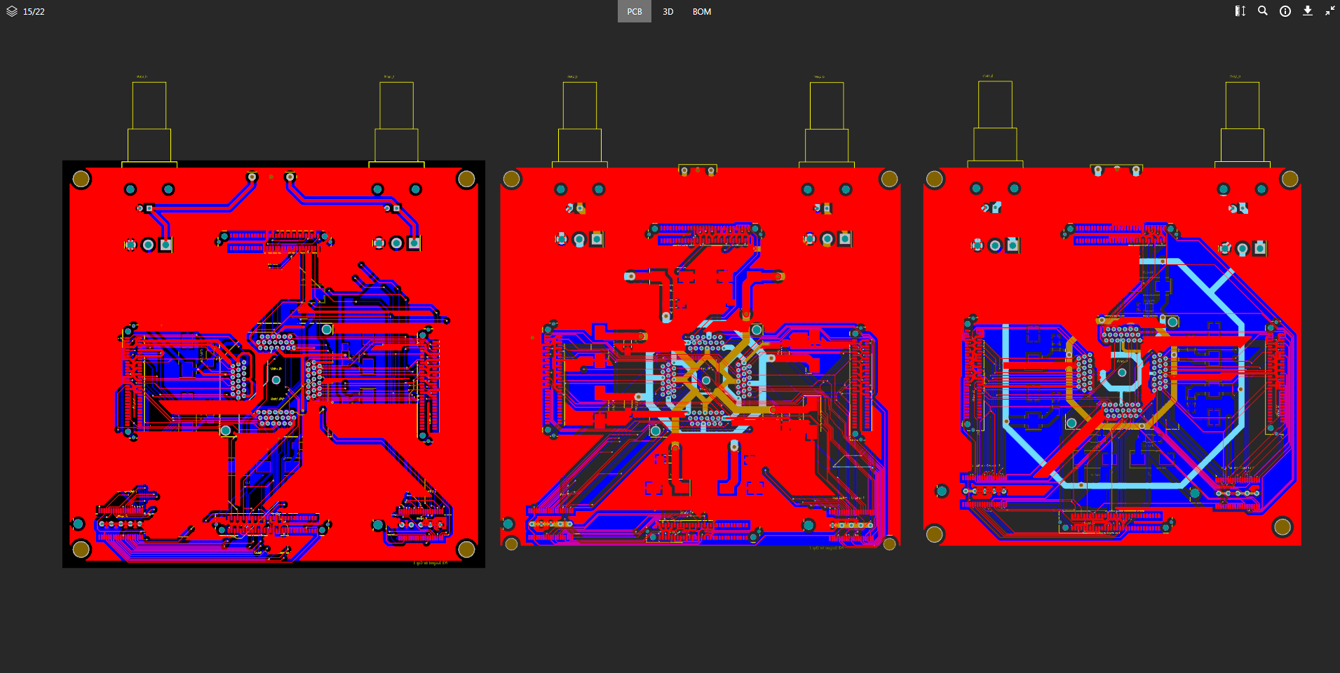
ChipOneTwoCombined is an open-source printed circuit board by chyavanphadke, from the chyavanphadke/University-Research-PCB-Design repository on GitHub. It is a 4-layer board of 333 × 109 mm with 81 parts on 490 nets, routed with 4,912 tracks and 445 vias.
PCB designed for a university project.
Specifications: 4 layered PCB that connects a custom designed chip with the Keysight Chip testing device
| Qty | Value | Footprint | References |
|---|---|---|---|
| 24 | 100uF | Capacitors_Tantalum_SMD:CP_Tantalum_Case-X_EIA-7343-43_Hand | CPchip1_C3, CPchip1_C4, CPchip1_C7, CPchip1_C8, CPchip1_C11, CPchip1_C12, CPchip1_C15, CPchip1_C16, CPchip2_C3, CPchip2_C4, CPchip2_C7, CPchip2_C8, CPchip2_C11, CPchip2_C12, CPchip2_C15, CPchip2_C16 +8 |
| 24 | 10uF | Capacitors_SMD:C_1206_HandSoldering | CPchip1_C1, CPchip1_C2, CPchip1_C5, CPchip1_C6, CPchip1_C9, CPchip1_C10, CPchip1_C13, CPchip1_C14, CPchip2_C1, CPchip2_C2, CPchip2_C5, CPchip2_C6, CPchip2_C9, CPchip2_C10, CPchip2_C13, CPchip2_C14 +8 |
| 12 | Y1247AstimulusGenerator | Y1247AstimulusGenerator:ERF8-030-05.0-L-DV-L-TR | CPchip1_U1, CPchip1_U2, CPchip1_U3, CPchip1_U4, CPchip2_U1, CPchip2_U2, CPchip2_U3, CPchip2_U4, CPchip3_U1, CPchip3_U2, CPchip3_U3, CPchip3_U4 |
| 6 | 3pinSwitchCustom | SW_MS12ANW03:SW_MS12ANW03 | CPchip1_U6, CPchip1_U10A1, CPchip2_U6, CPchip2_U11, CPchip3_U6, CPchip3_U10A1 |
| 6 | 5767007-8 | U4164AlogicAnalyser:TE_5767007-8 | CPchip1_J3, CPchip1_J4, CPchip2_J3, CPchip2_J4, CPchip3_J3, CPchip3_J4 |
| 4 | BNC | bnc_connector:TE_227161-1 | CPchip1_J1, CPchip1_J2, CPchip3_J1, CPchip3_J2 |
| 2 | Conn_Coaxial | bnc_connector:TE_227161-1 | CPchip2_J1, CPchip2_J2 |
| 1 | CPchip1_CHIP1 | chip1:280-5205-01 | CPchip1_U5 |
| 1 | CPchip2_CHIP2 | chip1:280-5205-01 | CPchip2_U5 |
| 1 | CPchip3_CHIP1 | chip1:280-5205-01 | CPchip3_U5 |
chyavanphadke/University-Research-PCB-Design
Specifications: 4 layered PCB that connects a custom designed chip with the Keysight Chip testing device

chyavanphadke/University-Research-PCB-Design
Specifications: 4 layered PCB that connects a custom designed chip with the Keysight Chip testing device

chyavanphadke/University-Research-PCB-Design
Specifications: 4 layered PCB that connects a custom designed chip with the Keysight Chip testing device

chyavanphadke/University-Research-PCB-Design
Specifications: 4 layered PCB that connects a custom designed chip with the Keysight Chip testing device

chyavanphadke/University-Research-PCB-Design
Specifications: 4 layered PCB that connects a custom designed chip with the Keysight Chip testing device

chyavanphadke/University-Research-PCB-Design
Specifications: 4 layered PCB that connects a custom designed chip with the Keysight Chip testing device

chyavanphadke/University-Research-PCB-Design
Specifications: 4 layered PCB that connects a custom designed chip with the Keysight Chip testing device

vsfteam/vsf
Versaloon Software Framework -- a tiny preemptive-capable event-driven incremental software framework for embedded systems

krishna-swaroop/KiCAD-Prism
Self-Hosted Web Application for displaying and interacting with KiCAD Projects

shilga/rp-gameboy-cartridge-hw
You should order with ENIG (electroless nickel immersion gold) plating. While the cartridge will work with HASL you will getter contact with ENIG and it is less prone to wearing down.

atomic14/esp32-tv-hardware
This is Work In Progress - I'm still working on this.

nataliethenerd/GCController23-0899D
Game Cube Controller 23-0899D reverse engineer


will127534/microSD-Switcher-Reader
A simple USB3.0 uSD card reader with a SD card switch for SBCs

protolux-electronics/soleil_hardware
Hardware design files for Soleil, an open source power management and sleep control board for Raspberry Pi
It measures 333 × 109 mm and has 4 copper layers, 1.6 mm thick.
81 parts. The full list of its parts is on this page, with links to each part's symbol and footprint where PCBKit's library has them.
From the chyavanphadke/University-Research-PCB-Design repository on GitHub, at the commit this page was made from: the board is chipOneTwoCombined/chipOneTwoCombined.kicad_pcb. PCBKit opens the board in the browser, with nothing to install.
Its repository states no licence, so its author keeps all rights: ask chyavanphadke before reusing the design.