
4 layers333 × 109 mm
ChipOneTwoCombined
chyavanphadke/University-Research-PCB-Design
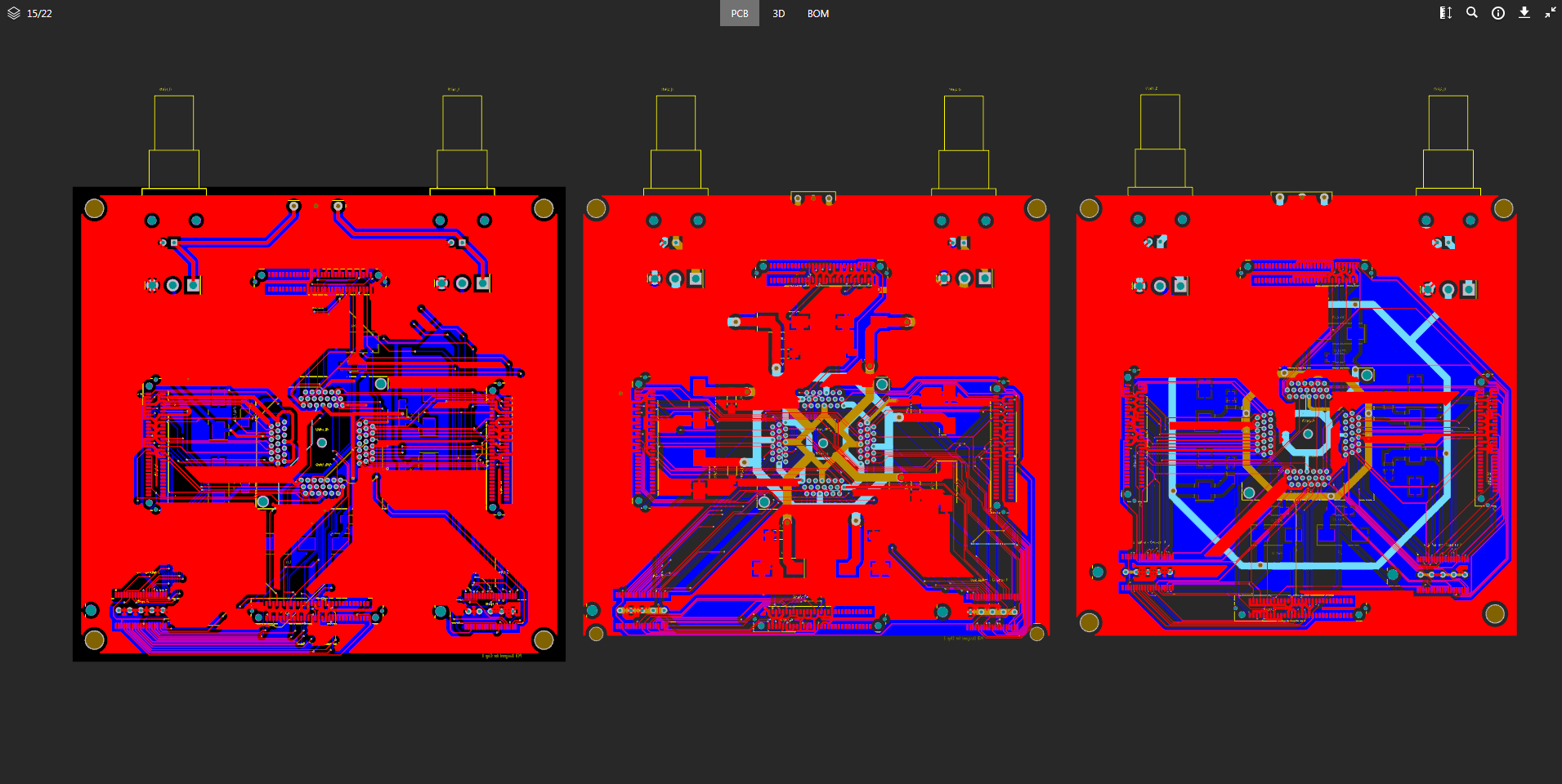
Specifications: 4 layered PCB that connects a custom designed chip with the Keysight Chip testing device
81 parts

Specifications: 4 layered PCB that connects a custom designed chip with the Keysight Chip testing device
ChipTwo is an open-source printed circuit board by chyavanphadke, from the chyavanphadke/University-Research-PCB-Design repository on GitHub. It is a 4-layer board of 111 × 105 mm with 27 parts on 181 nets, routed with 1,659 tracks and 126 vias.
PCB designed for a university project.
Specifications: 4 layered PCB that connects a custom designed chip with the Keysight Chip testing device
| Qty | Value | Footprint | References |
|---|---|---|---|
| 8 | 100uF | Capacitors_Tantalum_SMD:CP_Tantalum_Case-X_EIA-7343-43_Hand | CPchip2_C3, CPchip2_C4, CPchip2_C7, CPchip2_C8, CPchip2_C11, CPchip2_C12, CPchip2_C15, CPchip2_C16 |
| 8 | 10uF | Capacitors_SMD:C_1206_HandSoldering | CPchip2_C1, CPchip2_C2, CPchip2_C5, CPchip2_C6, CPchip2_C9, CPchip2_C10, CPchip2_C13, CPchip2_C14 |
| 4 | Y1247AstimulusGenerator | Y1247AstimulusGenerator:ERF8-030-05.0-L-DV-L-TR | CPchip2_U1, CPchip2_U2, CPchip2_U3, CPchip2_U4 |
| 2 | 3pinSwitchCustom | SW_MS12ANW03:SW_MS12ANW03 | CPchip2_U6, CPchip2_U11 |
| 2 | 5767007-8 | U4164AlogicAnalyser:TE_5767007-8 | CPchip2_J3, CPchip2_J4 |
| 2 | Conn_Coaxial | bnc_connector:TE_227161-1 | CPchip2_J1, CPchip2_J2 |
| 1 | CPchip2_CHIP2 | chip1:280-5205-01 | CPchip2_U5 |
chyavanphadke/University-Research-PCB-Design
Specifications: 4 layered PCB that connects a custom designed chip with the Keysight Chip testing device

chyavanphadke/University-Research-PCB-Design
Specifications: 4 layered PCB that connects a custom designed chip with the Keysight Chip testing device

chyavanphadke/University-Research-PCB-Design
Specifications: 4 layered PCB that connects a custom designed chip with the Keysight Chip testing device

chyavanphadke/University-Research-PCB-Design
Specifications: 4 layered PCB that connects a custom designed chip with the Keysight Chip testing device

chyavanphadke/University-Research-PCB-Design
Specifications: 4 layered PCB that connects a custom designed chip with the Keysight Chip testing device

chyavanphadke/University-Research-PCB-Design
Specifications: 4 layered PCB that connects a custom designed chip with the Keysight Chip testing device

chyavanphadke/University-Research-PCB-Design
Specifications: 4 layered PCB that connects a custom designed chip with the Keysight Chip testing device

pms67/HadesFCS
Complete flight control system designed from scratch. Hardware designed with KiCad.


loxodes/vna
Under development open hardware microwave vector network analyzer


MitkoDyakov/Calipatron
I design my own digital caliper based on STM32F103C8T6 blue pill.


alexbegoon/meshimi
Meshimi unlocks powerful mesh networking for your Flipper Zero combining Meshtastic, LoRaWAN and other protocols like Matter and Thread to give you rock‑solid connectivity across miles, even off‑grid.
It measures 111 × 105 mm and has 4 copper layers, 1.6 mm thick.
27 parts. The full list of its parts is on this page, with links to each part's symbol and footprint where PCBKit's library has them.
From the chyavanphadke/University-Research-PCB-Design repository on GitHub, at the commit this page was made from: the board is ChipTwo_oldDesign/ChipTwo.kicad_pcb. PCBKit opens the board in the browser, with nothing to install.
Its repository states no licence, so its author keeps all rights: ask chyavanphadke before reusing the design.