2 layers39.8 × 36.2 mm

 chislonljoseph/MCU-data-logger
MCU Data Logger PCB Design using KiCad
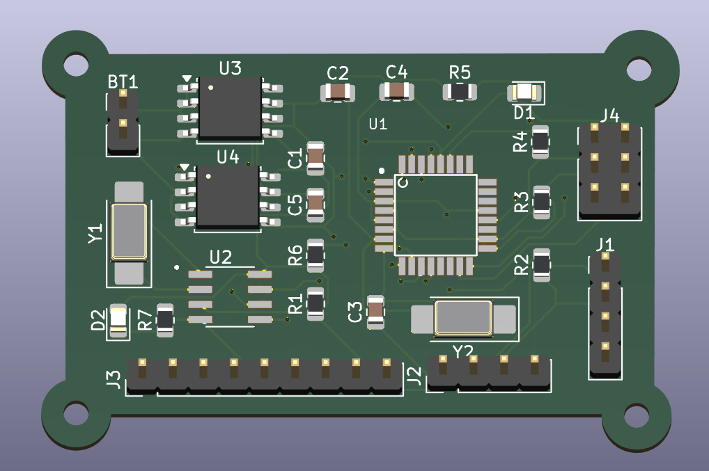
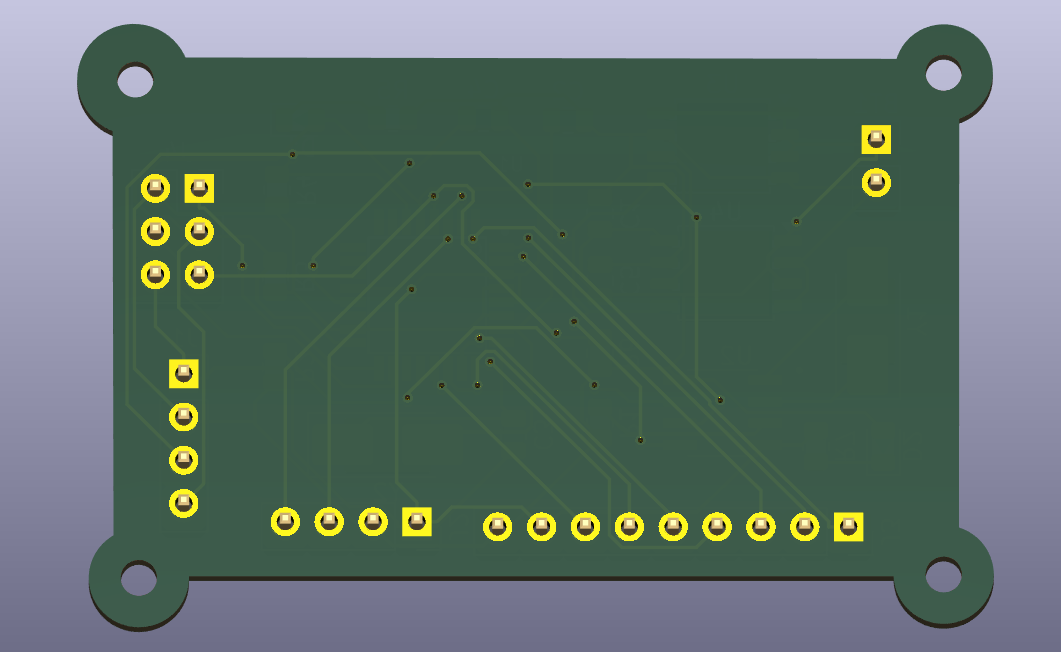
MCU data logger is an open-source printed circuit board by chislonljoseph, from the chislonljoseph/MCU-data-logger repository on GitHub. It is a 4-layer board of 51.2 × 34.3 mm with 29 parts on 33 nets, routed with 524 tracks and 25 vias.
It is built around the ATMEGA328P-AN, 24LC1025-I/P and DS1337S+T&R. Its parts include 7 resistors, 5 capacitors, 4 ICs, 4 connectors and 2 diodes. It belongs with the sensors and measurement boards and the AVR (ATmega, ATtiny) boards of this library.


A custom PCB designed in KiCad for an ATmega328P-based MCU Data Logger. This project demonstrates the complete PCB design workflow, from schematic capture and PCB layout to 4-layer stackup conversion and Gerber generation for fabrication.
This project includes:
| Component | Description |
|---|---|
| ATmega328P-AU | Main Microcontroller |
| DS1337S+ | Real-Time Clock (RTC) |
| 24LC1025 | EEPROM |
| 16 MHz Crystal | MCU Clock |
| 32.768 kHz Crystal | RTC Clock |
| LEDs | Status Indicators |
| Pin Headers | Programming & Communication |
| Battery Connector | Power Input |
| Parameter | Value |
|---|---|
| PCB Software | KiCad |
| Board Size | Approx. 127 × 96 mm |
| Initial Design | 2 Layers |
| Final Design | 4 Layers |
| Copper Pour | Yes |
| DRC Status | No Errors |
| Gerber Files | Generated |




MCU-data-logger/
│
├── Images/
├── Documentation/
├── Gerbers_4layers/
├── production/
├── Libraries/
├── MCU data logger.kicad_pcb
├── MCU data logger.kicad_sch
├── README.md
└── .gitignoreThe repository includes:
These files are located inside the Gerbers_4layers directory.
Through this project, I gained hands-on experience in:
Chislon L Joseph
B.Tech Electronics and Communication Engineering
Cochin University of Science and Technology (CUSAT)
This project is intended for educational and learning purposes.
| Qty | Value | Footprint | References |
|---|---|---|---|
| 4 | MountingHole | MountingHole:MountingHole_2.1mm | H1, H2, H3, H4 |
| 3 | 10k | Resistor_SMD:R_0805_2012Metric | R1, R2, R6 |
| 2 | 0.1uF | Capacitor_SMD:C_0805_2012Metric | C1, C4 |
| 2 | 22pF | Capacitor_SMD:C_0805_2012Metric | C2, C3 |
| 2 | 24LC1025 | Package_SO:SOIC-8_5.3x5.3mm_P1.27mm | U3, U4 |
| 2 | 330 | Resistor_SMD:R_0805_2012Metric | R5, R7 |
| 2 | 4.7k | Resistor_SMD:R_0805_2012Metric | R3, R4 |
| 2 | Conn_01x04_Pin | Connector_PinHeader_2.54mm:PinHeader_1x04_P2.54mm_Vertical | J1, J2 |
| 2 | LED | LED_SMD:LED_0805_2012Metric | D1, D2 |
| 1 | 100nF | Capacitor_SMD:C_0805_2012Metric | C5 |
| 1 | 16MHz | Crystal:Crystal_SMD_5032-2Pin_5.0x3.2mm_HandSoldering | Y2 |
| 1 | 32.768Khz | Crystal:Crystal_SMD_5032-2Pin_5.0x3.2mm_HandSoldering | Y1 |
| 1 | ATMEGA328P-AN | ATMEGA328P-AN:QFP80P900X900X120-32N | U1 |
| 1 | Battery | Connector_PinHeader_2.54mm:PinHeader_1x02_P2.54mm_Vertical | BT1 |
| 1 | Conn_01x09_Pin | Connector_PinHeader_2.54mm:PinHeader_1x09_P2.54mm_Vertical | J3 |
| 1 | Conn_02x03_Odd_Even | Connector_PinHeader_2.54mm:PinHeader_2x03_P2.54mm_Vertical | J4 |
| 1 | DS1337S_ | DS1337S_:SOIC127P600X175-8N | U2 |


wazzeemsha/ATMEGA328P-DataLogger-PCB
4-layer KiCad PCB design of an ATmega328P-AU based microcontroller data logger with dual EEPROMs, RTC, and complete manufacturing-ready Gerber files.


eldstal/touchless-xm
Physical buttons for media control on the Sony WH-1000XM2, WH-1000XM3, WH-1000XM4 and possibly WH-1000XM5 wireless headphones

futureshocked/KLP4e_MCU-Datalogger
This is the repository for the "MCU Datalogger" project.

futureshocked/KicadLikeAPro-Project-3-BACEE
This is one of the PCB projects from the Kicad Like a Pro book. It contains a two and four layer board that implements an Arduino clone with external EEPROM and a clock.

DevMajed/DataLogger-Board
Hardware PCB Design for AVR-based Datalogger using KiCAD
It measures 51.2 × 34.3 mm and has 4 copper layers, 1.6 mm thick.
29 parts, built around the ATMEGA328P-AN, 24LC1025-I/P and DS1337S+T&R. The full list of its parts is on this page, with links to each part's symbol and footprint where PCBKit's library has them.
From the chislonljoseph/MCU-data-logger repository on GitHub, at the commit this page was made from: the board is Kicad_Project/MCU data logger.kicad_pcb and its schematic Kicad_Project/MCU data logger.kicad_sch. PCBKit opens the board in the browser, with nothing to install.
Its repository states no licence, so its author keeps all rights: ask chislonljoseph before reusing the design.