2 layers82 × 62.5 mm

 cellularmitosis/atmega-gpib16
An ATmega-based GPIB-to-USB adapter board.
Atmega gpib is an open-source printed circuit board by cellularmitosis, from the cellularmitosis/atmega-gpib repository on GitHub, published under the MIT licence. It is a 2-layer board of 49.5 × 49.5 mm with 24 parts on 33 nets, routed with 236 tracks and 8 vias.
It is built around the ATMEGA168PA-PN and MCP2221A-I/P. Its parts include 8 capacitors, 5 resistors, 3 diodes, 3 connectors and 2 ICs. It belongs with the AVR (ATmega, ATtiny) boards of this library.


An ATmega-based GPIB-to-USB adapter board.
This board is untested.
Initial board design.
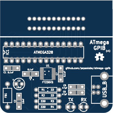
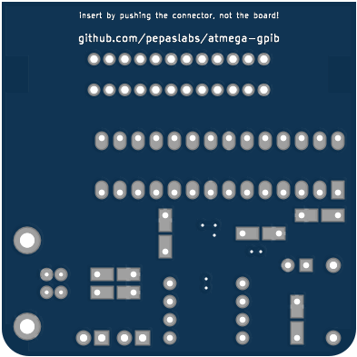
PDF.
This board design is Open-Source Hardware. It is licensed under the MIT License. It was designed by Jason Pepas.
Thanks to Steven Casagrande of Galvant Industries for releasing his GPIB-to-USB adapter as open source hardware. Using a few of his KiCAD footprints saved me a lot of time!
| Qty | Value | Footprint | References |
|---|---|---|---|
| 4 | 0.1uF | CERCAP_15_059B_0805 | C1, C7, C8, C9 |
| 3 | 330 | R_AXIAL_0W25_059A_PL | R3, R4, R5 |
| 2 | 33 | R_AXIAL_0W25_059A_PL | R1, R2 |
| 2 | 47pF | CERCAP_15_059B_0805 | C5, C6 |
| 1 | 10nF | CERCAP_15_059B_0805 | C2 |
| 1 | 10uF | ELCAP_10_20_V_059A | C3 |
| 1 | ATMEGA168PA-P | PL_DIP:DIP28_PL | IC1 |
| 1 | CONN_2X1 | SIL-2 | JMP1 |
| 1 | CONN_4X1 | SIL-4 | P1 |
| 1 | ERR | LED_3MM_069A | D3 |
| 1 | FERRITE | FERRITE_AXIAL_04_069A | FB1 |
| 1 | GPIB | 112-024-113R001 | P2 |
| 1 | MCP2221A | DIP14_PL | U1 |
| 1 | OSHW-logo_silkscreen-back_4mm | OSHW-logo_silkscreen-back_4mm | G*** |
| 1 | RX | LED_3MM_069A | D2 |
| 1 | TX | LED_3MM_069A | D1 |
| 1 | USB_B | USB_B | J1 |
It measures 49.5 × 49.5 mm and has 2 copper layers, 1.6 mm thick.
24 parts, built around the ATMEGA168PA-PN and MCP2221A-I/P. The full list of its parts is on this page, with links to each part's symbol and footprint where PCBKit's library has them.
From the cellularmitosis/atmega-gpib repository on GitHub, at the commit this page was made from: the board is kicad/atmega-gpib.kicad_pcb. PCBKit opens the board in the browser, with nothing to install.
Its repository publishes it under the MIT licence: you may reuse it on that licence's terms (keep the author's notice, and for a copyleft licence share your changes alike).

bigbass1997/PICTAS
Low-cost replay device for playing back Tool Assisted Speedruns on real hardware

obskyr/f-ramune
A device for testing and programming FRAM chips! Finally you can be sure that FRAM you bought from China works.

bigbass1997/remote64
Provides a method for N64 homebrew developers to test their roms on remote hardware


