
2 layers49.5 × 49.5 mm

 efe3535/AtmegaPCB
My Atmega PCB
AtmegaPCB is an open-source printed circuit board by efe3535, from the efe3535/AtmegaPCB repository on GitHub. It is a 2-layer board of 82 × 62.5 mm with 28 parts on 37 nets, routed with 204 tracks and 11 vias.
It is built around the ATMEGA168PA-PN. Its parts include 9 resistors, 8 diodes, 3 connectors, 2 capacitors and 1 IC. It belongs with the AVR (ATmega, ATtiny) boards of this library.
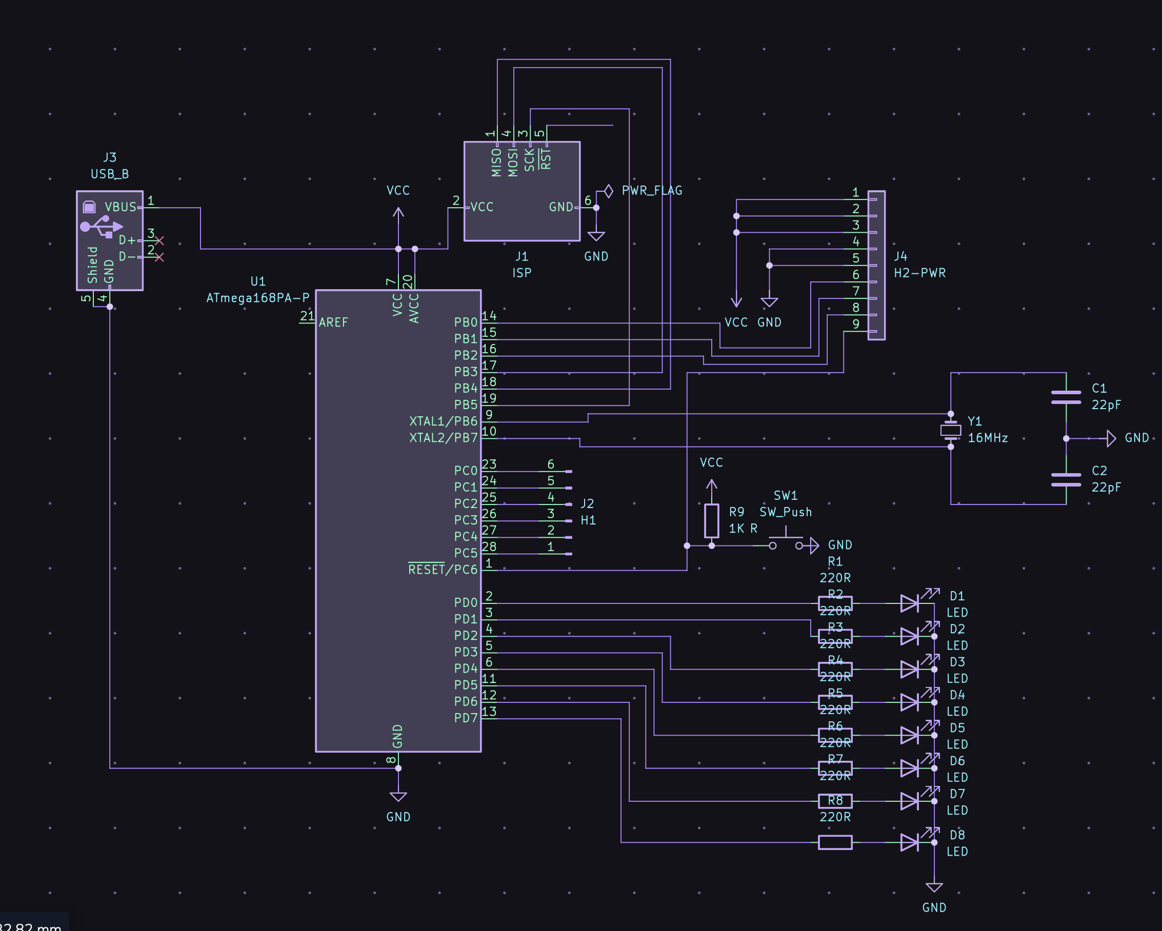
| Qty | Value | Footprint | References |
|---|---|---|---|
| 8 | 220R | Resistor_THT:R_Axial_DIN0207_L6.3mm_D2.5mm_P7.62mm_Horizontal | R1, R2, R3, R4, R5, R6, R7, R8 |
| 8 | LED | LED_THT:LED_D5.0mm_Horizontal_O1.27mm_Z3.0mm | D1, D2, D3, D4, D5, D6, D7, D8 |
| 2 | 22pF | Capacitor_THT:C_Axial_L3.8mm_D2.6mm_P7.50mm_Horizontal | C1, C2 |
| 2 | LOGO | footprints:aefeakyaziv2 | G***, G*** |
| 1 | 16MHz | Crystal:Crystal_HC49-4H_Vertical | Y1 |
| 1 | 1K R | Resistor_THT:R_Axial_DIN0207_L6.3mm_D2.5mm_P7.62mm_Horizontal | R9 |
| 1 | ATmega168PA-P | footprints:zif-28-pin | U1 |
| 1 | H1 | Connector_PinHeader_2.54mm:PinHeader_1x06_P2.54mm_Vertical | J2 |
| 1 | H2-PWR | Connector_PinHeader_2.54mm:PinHeader_1x09_P2.54mm_Vertical | J4 |
| 1 | ISP | Connector_PinHeader_2.54mm:PinHeader_2x03_P2.54mm_Vertical | ISP |
| 1 | SW_Push | Button_Switch_THT:SW_PUSH_6mm_H13mm | RESET |
| 1 | USB_B | Connector_USB:USB_B_OST_USB-B1HSxx_Horizontal | J3 |
It measures 82 × 62.5 mm and has 2 copper layers, 1.6 mm thick.
28 parts, built around the ATMEGA168PA-PN. The full list of its parts is on this page, with links to each part's symbol and footprint where PCBKit's library has them.
From the efe3535/AtmegaPCB repository on GitHub, at the commit this page was made from: the board is AtmegaPCB.kicad_pcb and its schematic AtmegaPCB.kicad_sch. PCBKit opens the board in the browser, with nothing to install.
Its repository states no licence, so its author keeps all rights: ask efe3535 before reusing the design.

joeycastillo/Sensor-Watch
A board replacement for the classic Casio F-91W wristwatch

TalismanDesign/PocketMage_PDA
An E-Ink PDA device using the ESP32 S3.

rusefi/rusefi
rusefi - GPL internal combustion engine control unit

hackclub/OnBoard
💡 Join 1,000 teenagers and make your first PCB with a $100 grant!

asterics/esp32_mouse_keyboard
ESP32 implementation for HID over GATT Keyboard and Mouse (Bluetooth Low Energy). Including serial API for external modules (similar to Adafruit EZKey HID)


Luos-io/luos_engine
Open-source and real-time orchestrator for cyber-physical-systems, to easily design, test and deploy embedded applications and digital twins.