2 layers86.4 × 38.1 mm
RTC8088
spark2k06/RTC8088
Real Time Clock for your PC XT. Very low profile, simple and open hardware.
11 parts33GPL-3.0

 cazacov/isa8_lpt_com_rtc1
ISA 8-bit Card with LPT, COM ports and real time clock
Isa8 lpt com rtc is an open-source printed circuit board by cazacov, from the cazacov/isa8_lpt_com_rtc repository on GitHub, published under the MIT licence. It is a 2-layer board of 99.1 × 10.2 mm with 26 parts on 121 nets.
It is built around the 74HCT245, 74HCT138D and DS12885N+. Its parts include 12 capacitors, 6 ICs, 2 connectors, 1 switch and 1 crystal. It belongs with the retro computing and games and lEDs and displays boards and the FPGA and CPLD boards of this library.


An 8-bit ISA expansion card providing a parallel port, two serial ports, and a battery-backed real-time clock for retro PC/XT systems.
The card was designed with a help of GitHub Copilot.
See prototype.md - Learn how to decode address, control RTC chip and design GAL firmware.
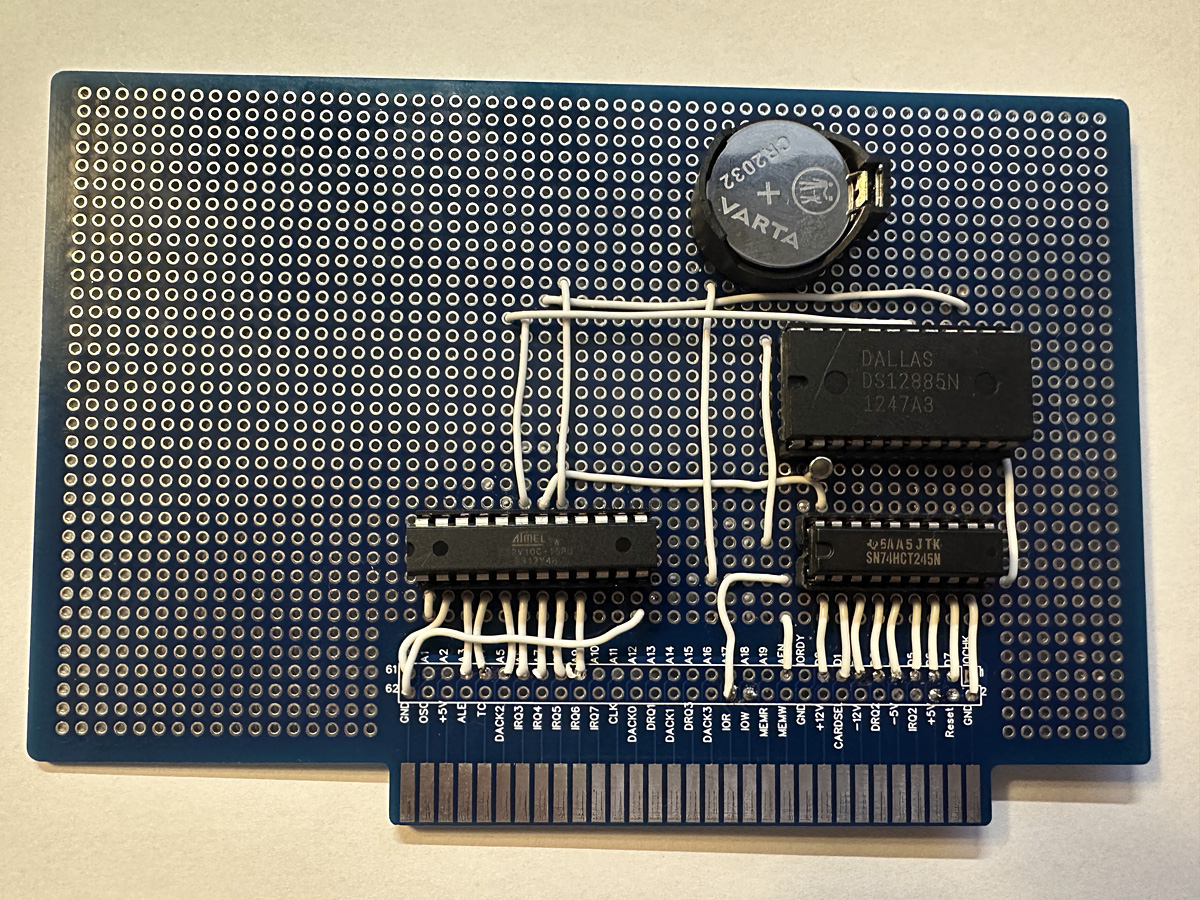 Vibe soldering with LLM.
Both ports use 16450/16550-compatible UARTs with RS-232 level shifting (GD75232N or equivalent). CS0 and CS1 are tied to GND; CS2 is the active-low chip select driven by the PLD.
| Port | Connector | Base Address Options | IRQ Options | CS Signal |
|---|---|---|---|---|
| COM1 | DB-9 | 0x3F8 or 0x2F8 | IRQ4 or IRQ3 | COM1_CS# |
| COM2 | 2×5 header | 0x3E8 or 0x2E8 | IRQ4 or IRQ3 | COM2_CS# |
| Ref | Frequency | Purpose |
|---|---|---|
| Y1 | 32.768 kHz | RTC crystal |
| Y2 | 1.8432 MHz | UART clock oscillator |
A 74HCT245 bidirectional transceiver decouples all peripheral data pins from the ISA bus:
A single ATF22V10 PLD decodes all port addresses and generates chip-select signals for every peripheral, plus the bus buffer enable and the RTC address strobe. No additional logic gates are required. Jumper inputs to the PLD allow per-device address and enable configuration.
See design.md for detailed PLD equations, pin assignments, and CUPL source.
| Jumper | Cap 1-2 (HIGH) | Cap 2-3 (LOW) |
|---|---|---|
| J1 (COM1 Addr) | 0x3F8 (COM1) | 0x2F8 (COM2) |
| J3 (COM2 Addr) | 0x3E8 (COM3) | 0x2E8 (COM4) |
| J5 (PRN Addr) | 0x378 (LPT1) | 0x278 (LPT2) |
| Jumper | Position 1 | Position 2 |
|---|---|---|
| J2 (COM1 IRQ) | IRQ4 | IRQ3 |
| J4 (COM2 IRQ) | IRQ4 | IRQ3 |
| J6 (PRN IRQ) | IRQ7 | IRQ5 |
| J7 (RTC IRQ) | IRQ2/9 / IRQ5 / IRQ6 / IRQ7 (1×5 header) | — |
J8 is a 2-pin header connected between DS12885 RCLR# (pin 21) and GND. The RCLR# pin has an internal pull-up inside the DS12885. Momentarily shorting J8 with a jumper cap (while the system is powered off) clears all CMOS RAM and RTC registers to defaults.
Devices are enabled/disabled by installing or removing the chip from its DIP socket. A 10k×8 pull-up resistor network on the 74HCT245 B-side ensures that empty sockets read as 0xFF, which is the expected response for absent I/O devices. Software detection (e.g., BIOS UART scratch register test) correctly identifies the device as absent.
The RTC is always enabled (no disable mechanism).
KiCad/V2/ISA8_LPT_COM_RTC.kicad_pro in KiCadKiCad/V2/ISA8_LPT_COM_RTC.kicad_schKiCad/V2/ISA8_LPT_COM_RTC.kicad_pcbThird party libraries should be stored in locations referenced with environment variables:
| Symptom | Check |
|---|---|
| Card not detected | ISA slot seating, power rails |
| Address conflicts | Reconfigure base address jumpers, ensure ATF22V10 firmware is programmed properly |
| IRQ conflicts | Change IRQ jumper settings |
| RTC loses time | Replace CR2032 battery |
| Serial errors | Baud rate, RS-232 cable/levels |
| Parallel port issues | Cable, port mode |
| File | Description |
|---|---|
KiCad/V2/ISA8_LPT_COM_RTC.kicad_pro | KiCad project |
KiCad/V2/ISA8_LPT_COM_RTC.kicad_sch | Schematic |
KiCad/V2/ISA8_LPT_COM_RTC.kicad_pcb | PCB layout |
design.md | Implementation plan — PLD equations, pin maps, CUPL source |
pld/ISA8_DECODE.pld | CUPL source for ATF22V10 |
pld/ISA8_DECODE.jed | Compiled JEDEC fuse map |
| Version | Notes |
|---|---|
| V2 | Current design iteration |
| V1 | Initial design (see KiCad/V1/) |
MIT
| Qty | Value | Footprint | References |
|---|---|---|---|
| 8 | 2200pF | Capacitor_THT:C_Disc_D5.0mm_W2.5mm_P5.00mm | C1, C2, C3, C4, C5, C6, C7, C8 |
| 3 | 0.1 uF | SKiselev:Cap_Cer_508 | C9, C11, C12 |
| 2 | 74HCT138 | Package_DIP:DIP-16_W7.62mm_Socket | U3, U4 |
| 1 | 10 uF | SKiselev:Cap_Elec_Radial_5mm_2.5mm | C10 |
| 1 | 10k | SKiselev:Conn_SIL5 | RN1 |
| 1 | 32768Hz | SKiselev:Crystal_32K_Horiz | Y1 |
| 1 | 74HCT245 | Package_DIP:DIP-20_W7.62mm_Socket | U2 |
| 1 | 82C11 | Package_DIP:DIP-40_W15.24mm_Socket | U1 |
| 1 | ATF16V8B | Package_DIP:DIP-20_W7.62mm_Socket | U5 |
| 1 | BUSPC_DEV | SKiselev:Conn_Edge_PCB_ISA8 | BUS1 |
| 1 | Battery_Cell | SKiselev:Battery_Holder_CR2032_Mouser_122-2420-GR | BT1 |
| 1 | Clear CMOS | Connector_PinHeader_2.54mm:PinHeader_1x02_P2.54mm_Vertical | JP1 |
| 1 | DS12885 | Package_DIP:DIP-24_W15.24mm_Socket | U7 |
| 1 | PRN | SKiselev:Conn_Dsub_DB25F | J1 |
| 1 | PRN_Conf | Connector_PinHeader_2.54mm:PinHeader_2x04_P2.54mm_Vertical | J2 |
| 1 | Switch_DIP_3_Positions | SKiselev:Switch_DIP_3_Positions | SW1 |
spark2k06/RTC8088
Real Time Clock for your PC XT. Very low profile, simple and open hardware.

markrvmurray/pico-thing
An 8-bit MC6809E / HD6309E single-board computer with a pair of Raspberry Pi Pico 2 (RP2350 / Pimoroni PGA2350) modules acting as intelligent bus peripherals, a 1–2 MB banked-RAM DAT/MMU, a 40-pin PATA hard-disk…

Toysoft/mb386sx-rc2016
The origin of this project is the M396F motherboard replica by Marco Both. Marco replicated the PCB layout of a certain revision of M396F motherboard. He didn't provide the schematic.

tebl/RC-ONE
A recreation of the MOS KIM-1 microcomputer, the start of the Commodore-line of computers. Complete with hex keypad, six digit displays and a lot of 8-bit fun!

crankery/crank68
One day I thought to myself I want to build a computer with the simplest 8 bit CPU I can think of". That CPU is the Motorola M6800 and this is the computer.


It measures 99.1 × 10.2 mm and has 2 copper layers, 1.6 mm thick.
26 parts, built around the 74HCT245, 74HCT138D and DS12885N+. The full list of its parts is on this page, with links to each part's symbol and footprint where PCBKit's library has them.
From the cazacov/isa8_lpt_com_rtc repository on GitHub, at the commit this page was made from: the board is KiCad/V1/ISA8_LPT_COM_RTC.kicad_pcb and its schematic KiCad/V1/ISA8_LPT_COM_RTC.kicad_sch. PCBKit opens the board in the browser, with nothing to install.
Its repository publishes it under the MIT licence: you may reuse it on that licence's terms (keep the author's notice, and for a copyleft licence share your changes alike).