4 layers40.9 × 87.5 mm

 cajunpanda/bluetooth-nes-advantage7
A bluetooth mod for the NES Advantage classic controller.
Bt nes advantage pcb is an open-source printed circuit board by cajunpanda, from the cajunpanda/bluetooth-nes-advantage repository on GitHub, published under the MIT licence. It is a 2-layer board of 78 × 36 mm with 45 parts on 48 nets, routed with 266 tracks and 32 vias.
It is built around the ESP32-WROOM-32E-N4, TPS63900DSKR and TP4056-42-ESOP8, with the CC0603KRX7R9BB104, DFE201610P-2R2M=P2 and AO3401A among its other parts. Its parts include 13 resistors, 10 capacitors, 4 diodes, 4 connectors and 3 ICs. It belongs with the retro computing and games and radio and wireless boards and the ESP32 boards of this library.


Integrated Bluetooth for the NES Advantage (NES-026) arcade stick. It pairs directly with a Nintendo Switch, an 8BitDo NES Retro Receiver (for a real NES), and PCs, phones, and emulators over BLE. No case cutting and no added buttons: everything runs from the stick's own controls, and it charges through the original cable hole.
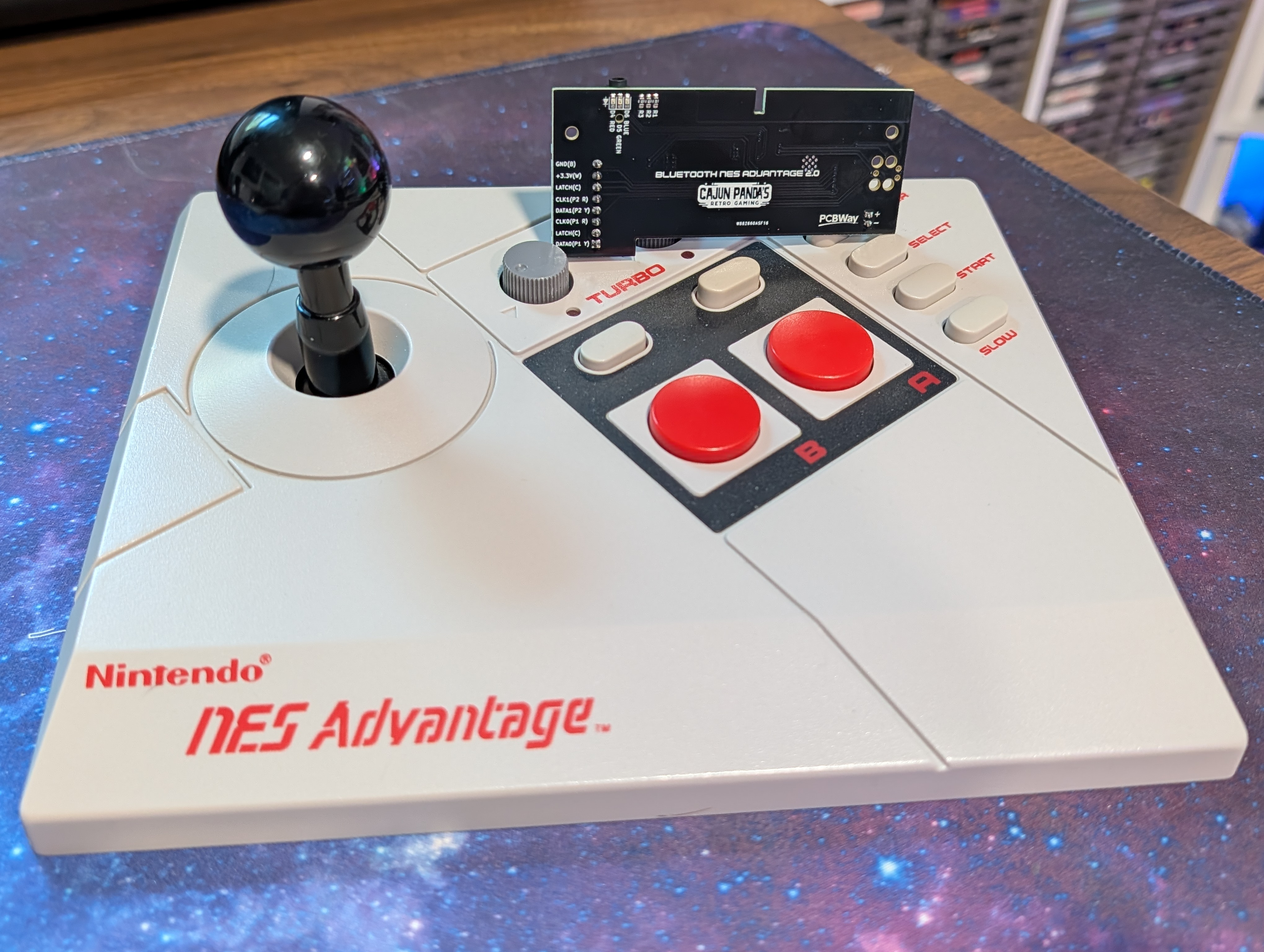
Watch the overview and how-to video for a tour of the mod and everything below in use.
A built-in Web Bluetooth app tests every input, tunes how the stick behaves, and flashes new firmware over the air with no cable and nothing to install. Put the stick in config mode (hold A + B + Select for 5 s), open the hosted config page in Chrome or Edge, and connect. Every button, the D-pad, the player-select slider, and the turbo dials light up live as you use them:
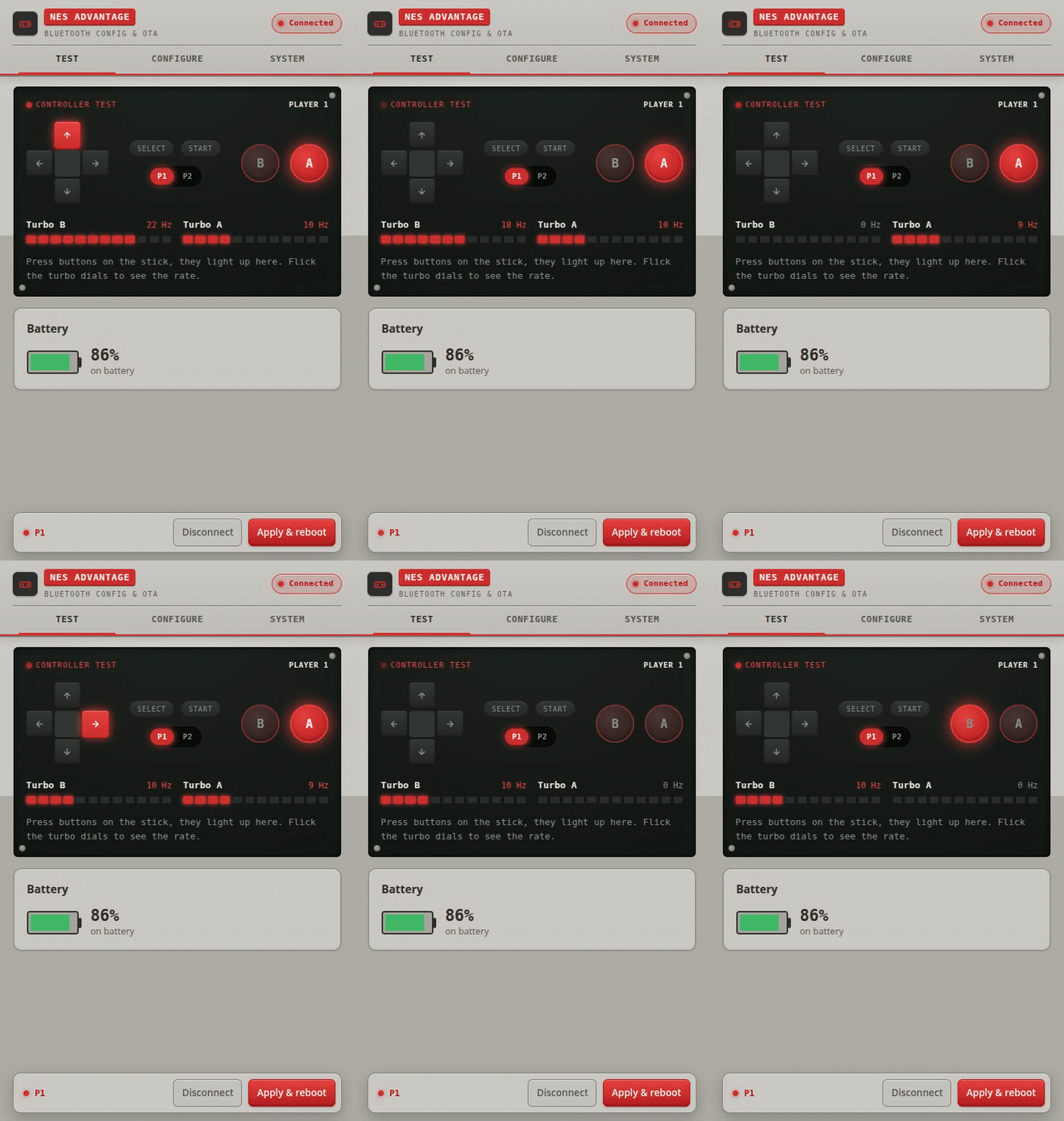
Change transport, button profile, and directional mode and apply over the air, or drop a
firmware.bin on the cartridge slot to update. The
manual has the full walkthrough.
A single custom PCB replaces the controller's cable. A bare ESP32-WROOM-32E reads the original CD4021 shift registers and presents the stick as a Bluetooth gamepad in one of two modes:
Turbo, slow motion, and the player-select slider all work as originally designed.
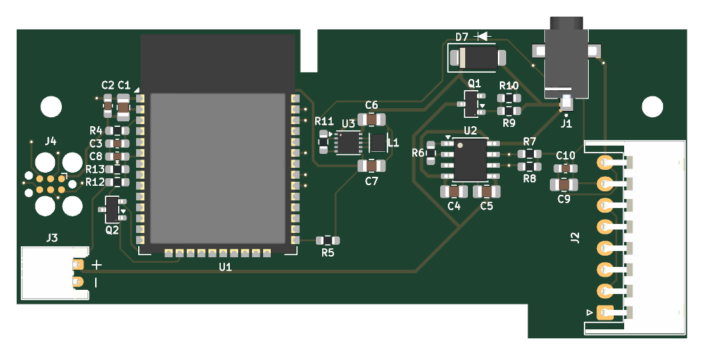
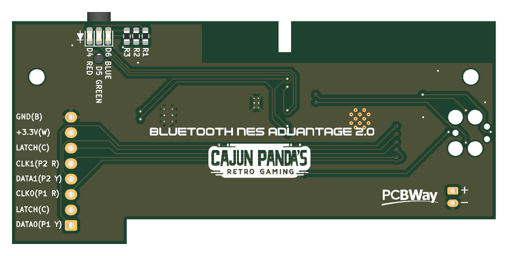
Start with the guide that fits you:
Complete kits and assembled boards are available at cajunpanda.com.
Questions and help: join the Discord.
| Path | Contents |
|---|---|
firmware/ | ESP-IDF dual-mode Bluetooth firmware |
hardware/ | KiCad PCB project and the 3D-printable jack plug |
web/ | Web Bluetooth config and OTA update page |
tools/ | Serial monitor and build helpers |
docs/ | Manual, install guide, hardware guide, firmware guide, protocol reference |
AGENTS.md | Working notes for contributors and AI coding agents |
Licensed by medium: firmware and software under MIT, hardware (PCB and 3D models) under CERN-OHL-P-2.0, documentation under CC-BY-4.0. See LICENSING.md.
The PCBs for this product are sponsored and produced by PCBWay. As always, their service was amazing and the fabrication as well as the shipping was fast. Because of the all-in-one customs and shipping price, the handling of taxes and other fees was very easy. Click here to order the PCBs from the shared project (gerbers preloaded).
This is an independent, unofficial project and is not affiliated with, endorsed by, sponsored by, or associated with Nintendo Co., Ltd. Nintendo, NES, Nintendo Entertainment System, NES Advantage, Nintendo Switch, and Nintendo Switch Pro Controller are trademarks of Nintendo. All trademarks are the property of their respective owners and are used here only for identification and compatibility. No Nintendo firmware, code, or assets are included; the Switch Pro Controller support is a clean-room implementation of the controller's publicly documented behavior, for interoperability only.
| Qty | Value | Footprint | References |
|---|---|---|---|
| 6 | 22µF | Capacitor_SMD:C_0603_1608Metric_Pad1.08x0.95mm_HandSolder | C1, C4, C5, C6, C7, C9 |
| 6 | Fiducial_0.5mm_Mask1mm | Fiducial:Fiducial_0.5mm_Mask1mm | FD01, FD02, FD03, FD05, FD06, FD07 |
| 5 | 10kΩ | Resistor_SMD:R_0603_1608Metric_Pad0.98x0.95mm_HandSolder | R4, R5, R7, R8, R9 |
| 4 | 100nF | Capacitor_SMD:C_0603_1608Metric_Pad1.08x0.95mm_HandSolder | C2, C3, C8, C10 |
| 3 | 1MΩ | Resistor_SMD:R_0603_1608Metric_Pad0.98x0.95mm_HandSolder | R10, R12, R13 |
| 3 | 200Ω | Resistor_SMD:R_0603_1608Metric_Pad0.98x0.95mm_HandSolder | R1, R2, R3 |
| 1 | 1.5kΩ | Resistor_SMD:R_0603_1608Metric_Pad0.98x0.95mm_HandSolder | R6 |
| 1 | 16.2kΩ | Resistor_SMD:R_0603_1608Metric_Pad0.98x0.95mm_HandSolder | R11 |
| 1 | 2.2µH | project_footprints:L_Murata_DFE201610P_HandSolder | L1 |
| 1 | 2N7002 | Package_TO_SOT_SMD:SOT-23 | Q2 |
| 1 | AO3401A | Package_TO_SOT_SMD:SOT-23 | Q1 |
| 1 | ESP32-WROOM-32E | RF_Module:ESP32-WROOM-32E | U1 |
| 1 | LTST-C193KGKT-5A | LED_SMD:LED_0603_1608Metric_Pad1.05x0.95mm_HandSolder | D5 |
| 1 | LTST-C193KRKT-5A | LED_SMD:LED_0603_1608Metric_Pad1.05x0.95mm_HandSolder | D4 |
| 1 | LTST-C193TBKT-5A | LED_SMD:LED_0603_1608Metric_Pad1.05x0.95mm_HandSolder | D6 |
| 1 | PJ-040-SMT-TR | project_footprints:CUI_PJ-040-SMT-TR | J1 |
| 1 | S2B-PH-K-S | Connector_JST:JST_PH_S2B-PH-K_1x02_P2.00mm_Horizontal | J3 |
| 1 | S8B-XH-A | Connector_JST:JST_XH_S8B-XH-A_1x08_P2.50mm_Horizontal | J2 |
| 1 | SS14 | Diode_SMD:D_SMA | D7 |
| 1 | TC2030 | Connector:Tag-Connect_TC2030-IDC-FP_2x03_P1.27mm_Vertical | J4 |
| 1 | TP4056 | Package_SO:SOIC-8-1EP_3.9x4.9mm_P1.27mm_EP2.29x3mm_ThermalVias | U2 |
| 1 | TPS63900 | Package_SON:WSON-10-1EP_2.5x2.5mm_P0.5mm_EP1.2x2mm_ThermalVias | U3 |
The 43 most common of 45 parts.

proegssilb/lightsaber-hardware
PCBs and other files for lightsaber soundboard hardware.


oresat/oresat-dxwifi-hardware
OreSat hardware for high speed data communications using 2.4 GHz WiFi.


Immortals-Robotics/MainBoard
Immortals main electronics for the Robocup Soccer Small-Size League

iandchasse/silkscreen-pcb
Silkscreen: open-hardware ESP32-S3 e-paper reader mainboard (KiCad 9). Formerly the de-link hub.

It measures 78 × 36 mm and has 2 copper layers, 1.6 mm thick.
45 parts, built around the ESP32-WROOM-32E-N4, TPS63900DSKR, TP4056-42-ESOP8 and CC0603KRX7R9BB104. The full list of its parts is on this page, with links to each part's symbol and footprint where PCBKit's library has them.
From the cajunpanda/bluetooth-nes-advantage repository on GitHub, at the commit this page was made from: the board is hardware/bt-nes-advantage-pcb/bt-nes-advantage-pcb.kicad_pcb and its schematic hardware/bt-nes-advantage-pcb/bt-nes-advantage-pcb.kicad_sch. PCBKit opens the board in the browser, with nothing to install.
Its repository publishes it under the MIT licence: you may reuse it on that licence's terms (keep the author's notice, and for a copyleft licence share your changes alike).